Download
1 / 2
21 likes | 60 Views
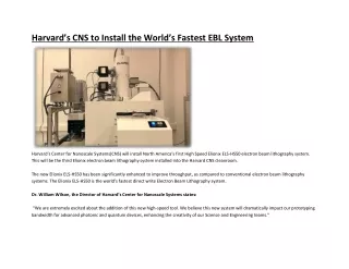
Harvardu2019s Center for Nanoscale Systems(CNS) will install North Americau2019s first High Speed Elionix ELS-HS50 electron beam lithography system. This will be the third Elionix electron beam lithography system installed into the Harvard CNS cleanroom.<br>

E N D
Harvard’s CNS to Install the World’s Fastest EBL System Harvard’s Center for Nanoscale Systems(CNS) will install North America’s first High Speed Elionix ELS-HS50 electron beam lithography system. This will be the third Elionix electron beam lithography system installed into the Harvard CNS cleanroom. The new Elionix ELS-HS50 has been significantly enhanced to improve throughput, as compared to conventional electron beam lithography systems. The Elionix ELS-HS50 is the world’s fastest direct write Electron Beam Lithography system. Dr. William Wilson, the Director of Harvard’s Center for Nanoscale Systems states: “We are extremely excited about the addition of this new high-speed tool. We believe this new system will dramatically impact our prototyping bandwidth for advanced photonic and quantum devices, enhancing the creativity of our Science and Engineering teams.”
The new high speed Elionix ELS-HS50 enables nanofabrication engineers to take advantage of the resolution benefits of electron beam lithography, while minimizing the inherent speed limitations of conventional vector scan electron beam lithography systems. The major features this system provides include: Up to 1000nA (1uA) Beam Current 10nm Beam Spot Size @ 100nA High position accuracy of 0.1nm pixel with 20bit DAC The Elionix ELS-HS50 electron beam lithography system design “bridges a gap”, between traditional electron beam resolution (nm scale) and other direct write lithography methods (um-mm scale). Writing tasks that have historically required using several lithographic methodologies, now can be written exclusively on the Elionix ELS-HS50 electron beam lithography tool. Nanofabrication engineers now can take advantage of the benefits of electron beam lithography, e.g. less line edge roughness, without sacrificing their need for speed. More information Elionix ELS-HS50 PDF Flyer> View & Download Original Source @ https://www.sts-elionix.com/harvards-cns-to-install-the- worlds-fasted-ebl-system/