Download
1 / 24
240 likes | 271 Views
Explore the results of an electrostatic simulation exercise to optimize the geometrical and electrical configuration of THGEMs for enhanced CsI Quantum Efficiency (QE) and low backscattering effect.

E N D
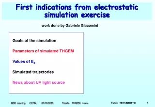
First indications from electrostatic simulation exercise work done by Gabriele Giacomini Goals of the simulation Parameters of simulated THGEM Values of Ez Simulated trajectories News about UV light source Fulvio TESSAROTTO
Electrostatic calculations are essential to optimize our THGEMs We decided to start from simple simulation exercises with ANSYS (and Garfield) in order to estimate the optimal geometrical and electrical configuration for the THGEM Critical points: • - Effective CsI Q.E. depends on the electric field at the CsI surface • - The backscattering effect depends on the gas and on the field too • The collection of photoelectrons in the holes for multiplication is • difficult to measure and critically depends on geometry and fields • The optimization of the THGEM geometry and operating parameters • will need some understanding, which can be achieved only • combining measurements and simulations Fulvio TESSAROTTO
MIP Edrift Relative E Ref. PC e E=0 E Reverse drift studies at Weizmann • Focusing is done by hole dipole field. • Maximum efficiency at Edrift =0 (like in GEM). • Slightly reversed Edrift (50-100V/cm) • good photoelectron collection & low sensitivity to MIPS (~5-10%) ! Attention: gas and field dependent! Fulvio TESSAROTTO
Electric field on photocathode surface created by the hole dipole field 0.4mm thick 0.3mm holes 0.7mm pitch DVTHGEM=2200V DVTHGEM=1200V DVTHGEM=800V DVTHGEM=2200V DVTHGEM=1200V DVTHGEM=800V Ref PC e >3kV/cm FIELD AT THE THGEM CsI SURFACE High field on the PC surface (high effective QE) Also at low THGEM voltages (e.g. in Ne mixtures!) Attention: varies with hole-pitch & hole-voltage C. Shalem et al. NIM A558 (2006) 468 Fulvio TESSAROTTO
Recent measurement by Elena Single THGEM, diam. 0.4 mm, th. 0.4 mm, pitch: 0.8 mm Fulvio TESSAROTTO
Photocurrent vs field on CsI not acceptable acceptable good Fulvio TESSAROTTO
The operational ΔV of THGEMs depends on gas Simulation performed using tools provided by RD51 Colleagues: based on “ANSYS” and “GARFIELD” Fulvio TESSAROTTO
Geometrical parameters of simulated THGEM Simulation performed by Gabriele Giacomini, using tools provided by Matteo Alfonsi and Gabriele Croci, based on ANSYS and GARFIELD Basic cell structure DEFAULT VALUES Thickness: 0.6 mm, Hole diameter: 0.4 mm, Pitch 0.8 mm, Rim: 0.0 mm, Cu thickness: 0.035 mm, Drift distance: 4.0 mm, (cont. plane) Induction dist.: 3.0 mm, (cont. plane) Induction field: 0.0 V/cm Drift field: 0.0 V/cm ΔV: 1500 V Fulvio TESSAROTTO
Values of Ez along the “z” axis, for different diameters Thickness: 0.6 mm, Pitch: 0.8 mm, Induction field: 0.0 V/cm Drift field: 0.0 V/cm hole scan along the “z” axis (hole axis) Fulvio TESSAROTTO
Values of Ez along the “y” axis, for different diameters Thickness: 0.6 mm, Pitch: 0.8 mm, Induction field: 0.0 V/cm Drift field: 0.0 V/cm diameter: 0.4 mm diam. hole Fulvio TESSAROTTO
Values of Ez along the “y” axis, for different pitches pitch: Thickness: 0.6 mm, Diameter: 0.4 mm, Induction field: 0.0 V/cm Drift field: 0.0 V/cm hole Fulvio TESSAROTTO
field values depend on: Thickness: Ez = Ez0 × (th0 / th) Hole diameter: non trivial (see slides) Pitch: non trivial (see slides) Rim: unknown Drift field: Ez = Ez0 + ED ΔV: Ez = Ez0 × ΔV / ΔV0 Max. V attained with th. = 0.2 mm ~ 900 V Max. V attained with th. = 0.4 mm: ~1400 V Max. V attained with th. = 0.6 mm: ~1700 V Fulvio TESSAROTTO
Values of Ez on the CsI surface for various diameters and pitches, compared with active area Ez ~ 1/ (pitch)4 Fulvio TESSAROTTO
Values of Ez on the CsI surface for various pitches and diameters, compared with active area Ez ~ exp(diam.) Fulvio TESSAROTTO
y x Photoelectron collection hole efficient collection area dead area Fulvio TESSAROTTO
trajectories for drift = 0 V/cm y x th. 0.6 mm, diam. 0.4 mm, pitch: 0.8 mm, ΔV = 1500 V y scan along the “x” axis scan along the “y” axis x Collection efficiency is o.k. Ez = - 543 V/cm 0 0.2 0.5 - 0.2 - 0.5 y Fulvio TESSAROTTO
trajectories for drift = -50 V/cm y x th. 0.6 mm, diam. 0.4 mm, pitch: 0.8 mm, ΔV = 1500 V y scan along the “x” axis scan along the “y” axis x partial collection efficiency Ez = - 593 V/cm “full collection radius” = 0.42 mm 0 0.2 0.5 - 0.2 - 0.5 y Fulvio TESSAROTTO
trajectories for drift = -500 V/cm th. 0.6 mm, diam. 0.4 mm, pitch: 0.8 mm, ΔV = 1500 V scan along the “x” axis low collection efficiency scan along the “y” axis Ez = - 1043 V/cm “full collection radius” = 0.33 mm 0 0.2 0.5 - 0.2 - 0.5 y Fulvio TESSAROTTO
trajectories for drift = +500 V/cm y x th. 0.6 mm, diam. 0.4 mm, pitch: 0.8 mm, ΔV = 1500 V y scan along the “x” axis scan along the “y” axis x Ez = - 43 V/cm Ez by far too low 0 0.2 0.5 - 0.2 - 0.5 y Fulvio TESSAROTTO
trajectories for drift = +500 V/cm y x th. 0.6 mm, diam. 0.4 mm, pitch: 0.8 mm, ΔV = 1500 V y scan along the “x” axis Loss of e- x scan along the “y” axis Ez = + 57 V/cm 0 0.2 0.5 - 0.2 - 0.5 y Fulvio TESSAROTTO
Consistency check with other simulation programs lattice spacing: 50 μm, 30 μm, 20 μm Fulvio TESSAROTTO
Consistency check with other simulation programs Fulvio TESSAROTTO
Main uses of UV light • UVA light (315 nm – 400 nm)is also called photochemical ray because many kinds of adhesives, fluorescence, and other chemistries react to UVA light. For the reason, its potential uses are uncountable, including UV curing/printing/coating, skin therapy, bank note detector, bio-weapon detector, air purification, etc • Applications: 1) UV curing systems, UV coating/printing assemblies for PVC, film, glass materials, and etc. 2) Security products such as Bank note detectors, Bio-weapon Detectors, Crime scene inspection, etc. 3) Phototheraphy devices to treat skin diseases including psoriasis, rickets, eczema, jaundice, and atopic dermatitis. 4) Automotive leak detector, Food checking. • UVB light (280 nm – 315 nm)is well known that UVB light exposures can be hazardous to human eyes and skin, but also UVB, often called as a dorno ray or a health ray, is assumed to be a beneficial to human health, UVB produces vitamin D in the skin, and prevent skin cancer caused by inefficient UVB exposure.Also in combinations of UVA (or by it self) UVB has become an increasingly popular and effective treatment for psoriasis, vitiligo, eczema, and other skin conditions. Most effective in case of psoriasis is UV light with wavelength of 311 nm • Applications: 1) Sterilization systems to purify water, surface, and air 2) Analysis of Minerals 3) EPROM Erasure 4) High Security UV marks • UVC light (200 nm – 280 nm) is also called germicidal ray. are the highest energy, most dangerous type of ultraviolet light. With that energy, it destroys DNA & PNA in microorganisms such as bacteria, viruses & mold, Thus, it generates Ozone.Especially 254.7nm is most effective wavelength for disinfections • Applications: 1) Water/Surface purification system 2) Laboratory testing devices Fulvio TESSAROTTO
LED at 255 nm Fulvio TESSAROTTO