Download

1 / 28
280 likes | 438 Views
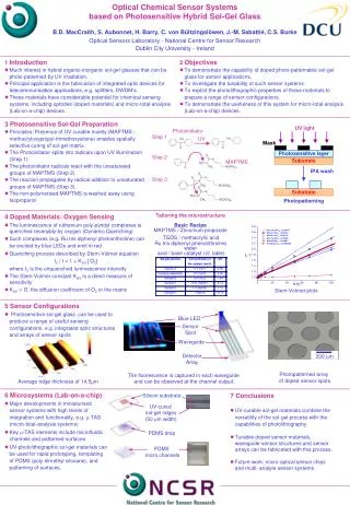
This study explores the innovative use of UV-patternable sol-gel technology in the fabrication of planar optical integrated circuits (PLCs). The research aims to enhance the efficiency and cost-effectiveness of optical communications by developing a waveguide fabrication process that operates at room temperature. The results demonstrate the successful incorporation of optical interconnects within a transmitter chip, focusing on optimizing refractive index tuning and overall device performance. This breakthrough could pave the way for next-generation optical networking solutions.

E N D
Planar Optical Integrated Circuits Based on UV-Patternable Sol-Gel Technology Jean-Marc Sabattié, Brian D. MacCraith, Karen Mongey, Jérôme Charmet, Kieran O’Dwyer, School of Physical Sciences, National Centre for Sensor Research, Dublin City University Mathias Pez, Francois Quentel,Thierry Dean THALES Research & Technology France
Plan • Introduction • Objectives • Sol-Gel Technology • Materials Preparation • UV-Patternable Sol-Gel Technology • Waveguide Fabrication Process • Parallel Optical Interconnects Assembly
Introduction • Increase in communications traffic larger capacity networks • Planar Lightwave Circuits (PLCs) as the future of optical communications: • Passive devices: Parallel Optical Interconnects (POI), Splitters, Couplers... • Active devices: Variable Optical Amplifiers...
overcladding Undercladding Core waveguide SiO2/GeO2 SiO2 Si or SiO2 Consolidation Photolithography and Reactive Ion Etching Flame Hydrolysis Deposition and Consolidation Introduction Current technology: silica-on-silicon technology • expensive steps • labour intensive • refractive index range limitations Flame Hydrolysis Deposition / Chemical Vapour Deposition
Objectives • Demonstration of the UV-patternable silica sol-gels technology for the manufacture of PLCs • at room temperature • at low cost • Example: parallel optical interconnects transmitter chip (POI Tx)
hn e- Objectives: Tx module Parallel connector Silicon Substrate Parallel waveguides Digital input Optical fibre ribbon Coupling optics wires Integrated circuit VCSEL array
Cladding Layer Guiding Layer Cladding Layer Silicon Substrate Waveguide Structure Targets 8-waveguides array sub-module to be integrated into a transmitter chip Constraints: • refractive indices are to match silica optical fibre parameters D (refractive index core - refractive index cladding) = 0.02
Catalyst Sol-Gel Technology • Silica/zirconia are made via the sol-gel process from Alkoxide Precursors Si(OR)4 + 2 H2O SiO2 + ROH Zr(OR’)4 + 2 H2O ZrO2 + R’OH Zirconia used for refractive index tuning
Refractive Index Tuning • Precursors for Cladding and Guiding Layers: • Tetrathyl orthosilicate (TEOS) • 3-(methoxysilyl)propyl methacrylate (MAPTMS) • Zirconium Propoxide • Irgacure 1800 (photoinitiator) • Methacrylic acid (complexing agent for Zr propoxide)
Refractive Index Tuning Dn = 0.01 for a 35 % concentration variation TEOS MAPTMS
Refractive Index Tuning Dn = 0.01 for a 6 % concentration variation Zr propoxide
Refractive Index Tuning Cladding and guiding materials preparation: • Same amount of TEOS and MAPTMS in both materials • to promote adhesion between layers • to obtain materials with similar thermal expansion coefficients • Refractive index difference (Dn) tuned by adjusting the Zirconium content
Hybrid UV-Patternable Sol-Gels MAPTMS or 3-(methoxysilyl)propyl methacrylate Resulting structure with a non-hydrolysable group as obtained with such precursors
Hybrid UV-Patternable Sol-Gels Aim: to create an organic network in parallel to the inorganic silica network by radical polymerisation non soluble in a wide range of solvents
UV Hybrid UV-Patternable Sol-Gels Photoinitiator MAPTMS
Photolithography Standard Mask-Aligner
Waveguide Preparation Process Spin-Coating cladding layer Spin-Coating cladding layer Thermal treatment Thermal treatment Spin-Coating guiding layer Dicing Waveguides UV-patterning Polishing facets Solvent wash Optical testing Thermal treatment
Refractive Index Tuning • UV-patterning step • Parameters: Intensity, Duration, Wavelength Effect of the UV exposure on the refractive index of the guiding layer materials
Waveguide Array Fabrication • Rinsing step Picture of ridge waveguides 3D-Map of ridge waveguides Acquisition with Dektak V 200 Si surface profiler
Waveguide structures • Characterisation of the waveguides Ridge profile of a ridge waveguide Cross-section picture of a waveguide Acquisition with Dektak V 200 Si surface profiler Acquisition with optical microscope
Waveguide Array Fabrication Conclusions • Compromise between • Refractive Index changes from • Precursors • UV-patterning • Thermal treatments • Hardness (for dicing, polishing) • Temperature resistance (for electronics bonding)
32.34 mm 35.16 mm 250 mm Optical Testing End view of two waveguides, light injected at the other ends Optical Loss = 0.79 dB/cm (measured at 840 nm by butt-coupling) Length of waveguides = ~1 cm
Tx module with connector Connector Waveguidearray Silicon Signal out Signal in Silicon Fibre Ribbon Laser array driving electronics VCSEL array 850 nm Alignment Pin
Tx module with connector Optical interface sub-module Fibre ribbon polished and metallized facet MT-ferrule VCSELs OE-component sub-assembly
POI Tx module testing Transmission tested at 2.5 Gbit/s/channel overall transmission rate: 20 Gbit/s perdevice
Conclusions • Parallel Optical Interconnect demonstrator • UV-patternable sol-gel materials technology for PLC applications demonstrated • Tunability of the materials for various applications (patterns, refractive index) • Compatibility with electronics industry methods
Brian D. MacCraith, Karen Mongey, Jérôme Charmet, Kieran O’Dwyer NCSR / School of Physical Sciences, Dublin City University Ireland Mathias Pez, Francois Quentel, Thierry Dean THALES Research & Technology France, Domaine de Corbeville, France Acknowledgements European Commission Brite-Euram Programme (Project number: BRPR-G98-0777).