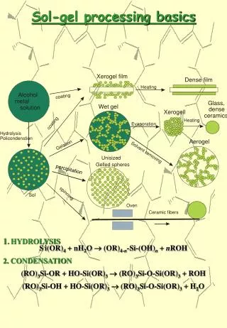
Download
1 / 22
240 likes | 459 Views
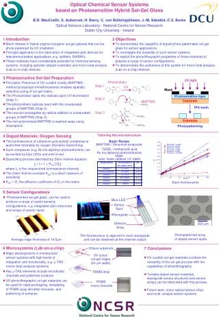
Multi-Analyte Optical Sensor Chip based on Photo-Patternable Hybrid Sol-Gel Integrated Optics. Jean-Marc Sabattié , Orla McGaughey, Aisling K. McEvoy, J é r ô me Charmet, Brian D. MacCraith. Outline. Introduction Doped sol-gel materials UV-patterned sol-gel waveguides Sensing mechanisms

E N D
Multi-Analyte Optical Sensor Chip based on Photo-Patternable Hybrid Sol-Gel Integrated Optics Jean-Marc Sabattié, Orla McGaughey, Aisling K. McEvoy, Jérôme Charmet, Brian D. MacCraith
Outline • Introduction • Doped sol-gel materials • UV-patterned sol-gel waveguides • Sensing mechanisms • Deposition process • Results • Conclusions / Future work
Introduction Development of a miniaturised multi-analyte sensor chip • Design: • novel configuration for efficient capture of fluorescence based on US Patent (US 6137117) – MacCraith et al. • Integration of • planar lightwave circuit technology (photo-patternable sol-gel waveguide structure). • Sol-gel sensor technology • Detection of O2 and CO2 analytes
Applications • Indoor air quality monitoring: • In-car comfort • Activates air-conditioning when O2 is below or CO2 is above a critical level • In-cabin comfort • Improve air conditions on flights • Blood gas analysis
Chip Design Blue LED Luminescent Sensor Spots (doped sol-gel sensor materials) Waveguide Series (UV-patternable sol-gel) Detector Array
Catalyst Sol-Gel Materials • Doped sol-gel materials: • Tetrathyl orthosilicate (TEOS) • Methyltriethyl orthosilicate (MTEOS) inert porous inorganic silica matrix for sensor immobilisation Si(OR)4 + 2 H2O ROH + SiO2 • hydrolysis • condensation
UV-Patternable Sol-Gel Materials • UV-patternable sol-gel material • TEOS • Zirconium propoxide (ZrOP) • 3-(methoxysilyl)propyl methacrylate (MPTS) • Photoinitiator
Catalyst Zr(OR’)4+ 2 H2OZrO2+ R’OH UV-Patternable Sol-Gel Materials Zirconia used for refractive index tuning Total internal reflection nair = 1 nguiding ncladding
UV-Patternable Sol-Gel Materials • to create an organic network cross-linked to the inorganic silica/zirconia network by radical polymerisation • non soluble in a wide range of solvents
UV UV-Patternable Sol-Gel Materials Photoinitiator MPTS
Photolithography Standard Mask-Aligner
Ridge Waveguides Picture of ridge waveguides 3D-map of ridge waveguides
Ridge Waveguides Cross-Sections Ridge Waveguides Air 10 mm Cladding Layer 30 mm Silicon Substrate
O2 sensor : [Ru(dpp)3]Cl2 Ruthenium-tris(4,7-diphenyl-1, 10-phenanthroline) dichloride Oxygen Sensing lexc = 470 nm lem = 610 nm Fluorescence quenching described by Stern-Volmer equation
Carbon Dioxide Sensing • CO2 sensor: HPTS (pH indicator) 8-hydroxy-1,3,6-pyrenetrisulfonate salt • in solution, equilibrium acid form base form • production of acid in solution by dissolution of CO2 • acidity changes the concentration of the conjugate base • specific excitation of the conjugate base at 470 nm • collection of emission at 525 nm
Multi-Analyte Simultaneous Sensing Excitation source: Single Blue LED Detector: Linear Detector Array 470 nm 525 nm 610 nm
Sensor Deposition Techniques Soft-lithography • polydimethylsiloxane (PDMS) stamp • To achieve: • better control of the drop size • reproducibility Pin-printing • metal pin Ink-jet printing • print-head
Initial Results - Oxygen CCD image 200 mm separation between the waveguides Intensity profile
Initial Results - Oxygen Stern-Volmer plot • High sensitivity for low concentrations • 0 -100 % detectable range • Sensitivity tuned by sol-gel formulation
Conclusions • Demonstration of an oxygen multi-channel sensor chip • patterning of a series of waveguides • simultaneous detection of the luminescence produced by Ru(dpp)3 in each waveguide
Future work • Optimisation of the design parameters • dimension and refractive index of the waveguides • Optimisation of the printing method • to allow for deposition of CO2 and O2 sensor spots of specific diameter and thickness • Demonstration of a miniaturised portable multi-analyte sensor with RF communications
Orla McGaughey Aisling McEvoy Jérôme Charmet Brian D. MacCraith Enterprise Ireland Funding under Research Innovation Fund IF/2002/353 Optical Sensors Laboratory, National Centre for Sensor Research, Dublin City University, Ireland Acknowlegdements