Upgraded Charge Sensitive Preamplifier
230 likes | 254 Views
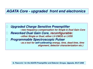
AGATA Core - upgraded front end electronics. Upgraded Charge Sensitive Preamplifier - new frequency compensation for Single & Dual Gain Core Reworked Dual Gain Core, reconfigurable: - either Single or Dual; either LV-CMOS or LVDS

Upgraded Charge Sensitive Preamplifier
E N D
Presentation Transcript
AGATA Core - upgraded front endelectronics Upgraded Charge Sensitive Preamplifier -new frequency compensation for Single & Dual Gain Core Reworked Dual Gain Core, reconfigurable: -either Single or Dual; either LV-CMOS or LVDS Programmable Spectroscopic Pulser -as a tool for self-calibrating energy, time, dead time, time alignment, detector characterization etc.) G. Pascovici for the AGATA Preamplifier and Detector Groups, Uppsala, 09.07.2008
Motivation, going on work… • Follow-up on previous AGATA Week presentations: - Wiring and Frequency Compensations, B. Bruyneel and G. Pascovici, Orsay, 2007 - Dual Gain Core (e.g. with 5 MeV and 20 MeV ranges) Dino Bazzacco’s request, Aug. 2007 - ToT Method (calibration and measurements), Francesca Zocca et al, Padova, 2007
Transfer function at high frequency range Dominant pole compensation See presentations of B. Bruyneel & G. Pascovici @ AGATA Week, Orsay, Jan, 2007 • Return GND concept • for single & triple cryostat • Wires – inductivities …
Issue: Front-End Electronics & wiring in cryostat Cold partWarm part Core return GND Cold partWarm part
AGATA Single & Dual Gain Core reworked frequency compensations tested with AGATA_Dummy-3D internal network compensation Lead comp. (1. OpAmp) Cryostat wiring as part of the front-end electronics external network compensation - minimum Miller effect (min.) - lead compensation (min.) - lead-lag compensation (adj.) - dominant pole compensation (adj.) AGATA Dummy 3Dcapsule + wiring
AGATA Single & Dual Gain Core reworked frequency compensations internal network compensation Lead comp. (1. OpAmp) Cryostat wiring as part of the front-end electronics external network compensation - minimum Miller effect (min.) - lead compensation (min.) - lead-lag compensation (adj.) - dominant pole compensation (adj.)
AGATA Single and Dual Core frequency compensations tr ~ 30-40 ns Multiple frequency compensations: - minimum Miller effect - lead compensation - lead-lag compensation - dominant pole compensation * without dominant pole & lead-lag compensation networks * implemented dominant pole & lead-lag compensation network • Comments: • Stability criteria not only oscillations, • rather it is circuit performance as • exhibited by peaking and ringing • the method of compensation depends • on the equivalent op amp type and • feedback, source and load networks tr ~ 25 - 30 ns a HF rejection with almost no extra “price” paid for rise time !
Dual Core in ‘GP -Cryostat’ (cold) • Dual Corein‘GP - Cryostat’ (cold) • cryostat equipped with AGATA cold parts • and wiring (only 1.8 Ohm, no 48.5 Ohm!) tr ~ 26.8 ns Ch.1 @ ~ 800 mV ~ 25.6 ns Ch.2 @ ~ 220 mV • Equivalent resolutions (if cold Cf ~1pF) • Ch1 ~ 1.15 keV @ ~ 150 keV • Ch2 ~ 1.25 keV @ ~ 150 keV • (6 µs shaping time Ortec 671 & IKP-MCA) • rise time ~ 26 -29 ns (+/- 2ns 10mV-1V) • no overshoots & undershoots • NB: flat top of ~ 500 ns (PSA peaking) tr ~ 29.2 ns Ch.1 @ ~ 220 mV ~ 29.2 ns Ch.2 @ ~ 60 mV
AGATA Single / Dual Gain Core Final Specifications • news - core front-end • Single or Dual Gain • Extended range~180 MeV • (both single and dual gain) • LV-CMOS or LV-DSfor the • INH-Ch1, INH-Ch2 and • Pulser Trigger-In • LV-CMOS for SHDN and • Pulser DAC CNTRL lines • Up-dated frequency • compensation for cryostat • wiring (dominant pole comp)
Time over Threshold (ToT) method See Francesca Zocca, AGATA Week, Padova, Nov. 2007; FreeDAC Workshop, Ljubljana, Mai, 2008
Fast Reset as tool to implement the “TOT” method Analog Mode + DT1 Active Reset – OFF Fast Reset circuitry ToT ~ DT2 Active Reset – ON • very fast recovery from TOT mode of operation • fast comparator LT1719 (+/- 6V) • factory adj. threshold + zero crossing • LV-CMOS (opt) • LVDS by default
Dual Gain Core -the upgraded features and its structure • Linear Range: 2keV -180 MeV (far beyond the ADC limit !) • Two modes of operations: • a)Pulse Amplitudeb)Time Over Threshold(ToT) • (0-5 MeV); (0-20 MeV)(5-180 MeV); (20-180 MeV) cold part warm part Ch 1 ~ 200 mV / MeV C-Ch1 /C-Ch1 INH1 SDHN1 Pole /Zero Adj. Fast Reset (Ch1) Differential Buffer (Ch1) Common Charge Sensitive Loop + Pulser + Wiring 36_fold segmented HP-Ge detector + cold jFET one MDR 10m cable Ch 2 ~ 50mV / MeV C-Ch2 /C-Ch2 INH2 SDHN2 Pole /Zero Adj. Fast Reset (Ch2) Differential Buffer (Ch2) Single Core or Dual Core wiring FADC Programmable Spectroscopic Pulser Pulser CNTRL
Time over Threshold [ToT] method F. Zocca, AGATA Week Padova, Nov., 2007 Time over Threshold Analog Core Ch.1 Core Ch.1 Reset Threshold Ch.1 Analog Time over Threshold Core Ch.2 Core Ch.2 Reset Threshold Ch.2 5 MeV 20 MeV 180 MeV
Issue: INH-C1 and Core Ch2 X-talk on the transmission line due to INH-C1 return GND … X-talk ~ 9 mV (~ slow signals) • keeping INH-C as LV-CMOS • digital signal • Advantage: • -simple upgrade of the single • gain core to dual gain core • Disadvantage: • - relativelarge crosstalk INH-C1 and 2.nd core signal • INH-C1 Core_Ch2 X-talk ~ 15 mV (~ fast signals)
AGATA Dual_Core LVDS transmission of digital INH and Pulser_In signals AGATA Dual Core crosstalk test measurements Ch2 (analog signal) vs. LVDS-INH-C1 (bellow & above threshold) Core amplitude just below the INH threshold Core amplitude just above the INH threshold Ch1@ INH_Threshold - (~ 4mV) Ch1 @ INH_Threshold + (~ 4mV) Ch2 @ INH_Threshold + (~ 1mV) Ch2@INH_Threshold + (- 1mV) LV_CMOS LV_CMOS INH_Ch1/+/ INH_Ch1/-/ tr ~ 1.65 ns INH_Ch1/+/ tf ~ 2.45 ns INH_Ch1/-/ (1) Core_Ch1, (2) Core_Ch2, (3) INH_Ch1(LVDS/-/, (4) INH_Ch1(LVDS/+/) G.Pascovici, Dual_Core IReS Test Box, warm jFET, Feb.23, 2008
Dual Core in ‘GP-Cryostat’ (cold) 5 & 10 m LVDS transmission line Trigger tin ~ 1.0 ns tr ~ 26.8 ns Ch.1 @ ~ 800 mV ~ 25.6 ns Ch.2 @ ~ 220 mV 5m cable tr, tf ~ 1.5 ns 10 m cable tr, tf ~ 1.5 ns ~ 22ns / 5m • Resolutions: • Ch1 ~ 1.15 keV @ ~ 150 keV • Ch2 ~ 1.25 keV @ ~ 150 keV • (6 µs shaping time Ortec 671 & IKP-MCA) • Rise time ~ 26-29 ns • NO overshoots & undershoots • Pulse shape: flat top of ~ 500 ns tr ~ 29.2 ns Ch.1 @ ~ 220 mV ~ 29.2 ns Ch.2 @ ~ 60 mV
Rework to be done in the FADCs LV-CMOS to LVDS LVDS to LV-CMOS tin ~ 1.0 ns tr, tf ~ 1.5 ns 10m cable + 1.22V Tiny converter PCBs to be installed in the FADCs LVDS- TX LVDS- RX (2x)
Dual Gain Core -the upgraded features and its structure • Linear Range: 2keV -180 MeV (far beyond the ADC limit !) • Two modes of operations: • a)Pulse Amplitudeb)Time Over Threshold(ToT) • (0-5 MeV); (0-20 MeV)(5-180 MeV); (20-180 MeV) cold part warm part Ch 1 ~ 100 mV / MeV C-Ch1 /C-Ch1 INH1 SDHN1 Pole /Zero Adj. Fast Reset (Ch1) Differential Buffer (Ch1) Common Charge Sensitive Loop + Pulser + Wiring 36_fold segmented HP-Ge detector + cold jFET one MDR 10m cable N.B. The dual gain core can be configured also as a Single Core with LV-CMOS digital signals Ch 2 ~ 50mV / MeV C-Ch2 /C-Ch2 INH2 SDHN2 Pole /Zero Adj. Fast Reset (Ch2) Differential Buffer (Ch2) Single Core or Dual Core wiring FADC Programmable Spectroscopic Pulser Pulser CNTRL
Potential use of PSPfor self-calibrating ParameterPotential Use / Applications • Pulse amplitudeEnergy, Calibration, Stability • Pulse FormTransferFunction in time (rise time, fall time)domain, ringing (PSA) • Detector Bulk Capacities Crosstalk input data (also for Dummy Capacities)(Detector characterization) • Pulse FormTOT Method (PSA) • Repetition Rate (c.p.s.) Dead Time(Efficiency meas.) (with periodical or statistical distribution) • Time alignment Correlated time spectra • Segments calibration points Low energy calibration points Alignment of segment signals
Pulser Mode of operation Pulser Specs and Measurements • Dynamic range: - Core 0 to ~ 180 MeV (opt. ~ 90 MeV) - Segments 0 to ~3 MeV (opt. ~ 1 MeV) • Rise Time Range: 20 ns - 60 ns (by default ~45 ns) • Fall Time Range: 100 µs - 1000 µs (by default ~150 µs) • Long Term Stability: < 10 / 24 h - 4
Measurements: • GSI Single Cryostat (Detector S001) • Portable 16k channels MCA (IKP) • Resolution (acquisition time 12-14h): • - core 1.08 keV Pulser (Detector) • - cold dummy (V3): 0.850 keV • - segment Pulser: < 0.90 keV • - core @ 59.5 keV: 1.10 keV • - core @ 122.06 keV: 1.15 keV
Conclusions • A very low noise, very wide dynamic range • charge-sensitive pre-amplifier has been • developed and tested to be used with a • highly segmented and encapsulated HP-Ge • AGATA Detector • Furthermore its wide spectroscopic range • has been successfully extended by more • than one order of magnitude, by switching • (below the maximum of the ADC range) from • the standard amplitude spectroscopic • method to the new TOT technique • - two modes of operations four sub-ranges, • namely: 0-5 (20) MeV and 5(20)-180 MeV • A very clean transfer function at very high • counting rates and adverse cryostat wiring • (useful set of 2D & 3D “Dummy - detectors”) • An accurate Programmable Spectroscopic • Pulser has been developed and imple- • mented in the AGATA front-end electronics
Conclusions Single Core Dual Core • A very low noise, very wide dynamic range • charge-sensitive pre-amplifier has been • developed and tested to be used with a • highly segmented and encapsulated HP-Ge • AGATA Detector • Furthermore its wide spectroscopic range • has been successfully extended by more • than one order of magnitude, by switching • (below the maximum of the ADC range) from • the standard amplitude spectroscopic • method to the new TOT technique • - two modes of operations four sub-ranges, • namely:0-5 (20) MeV and 5(20)-180 MeV • A very clean transfer function at very high • counting rates and adverse cryostat wiring • (useful set of 2D & 3D “Dummy - detectors”) • An accurate Programmable Spectroscopic • Pulser has been developed and imple- • mented in the AGATA front-end electronics Floating motherboard Floating motherboard Triple Ganil Triple Milano Floating motherboard Floating motherboard Triple Cryostat, one set of 12+1 warm CSPs