Download
1 / 26
290 likes | 365 Views
Learn about efficient VHDL coding practices for FPGA design from Xilinx Workshop EE514. Explore hierarchical design, synchronous circuits, asynchronous design case studies, and tips for clock skew reduction. Discover the importance of global buffers and clock dividers.

E N D
File types and file I/O ROM model Bi-directional pad model Attribute declaration and attribute specification Access and record type Guarded block Guarded signal and null waveform Disconnection specification Writing efficient VHDL code Exercises FPGA Design Techniques from Xilinx Workshop EE514
Top Level of Design Infer or instantiate I/O here State Machines Data Paths One-hot Pipelining Binary Muxing/De-muxing Enumerated Arithmetic Counters Building Blocks Adders/Subtractors Standard widths Bit Shifters Pipeline RAMs Accumulators Specific Functions Logiblox RAM Other IP/Cores Coregen FIFOs Parametizable functions FIR Filters RAM Technology Specific Functions Hierarchical Design • Using Hierarchy leads to easy design readability, re-use, and debug EE514
Design Entry Methods • Use HDL for: • State machines • Control logic • Bussed functions • Use schematics for: • Top level design • Manually optimized logic • “Mixed mode” designs utilize the best of both worlds
Design Readability • Choose hierarchical blocks that have: • Minimal routing between blocks • Logical data flow between blocks • Choose descriptive labels for blocks and signals • Keep clock domains separated • Makes the interaction between clocks very clear • Each block should be less than 400 lines of HDL code • Easier to read, synthesize, and debug
Design Reuse • Build a set of blocks that are available to all • Register banks • FIFOs • Other standard functions • Custom functions commonly used in your applications • Name blocks by function and target technology • Easy to locate the block you want • Example: REG_4X8_SP (bank of four 8-bit registers, targeting Spartan) • Store in a separate directory
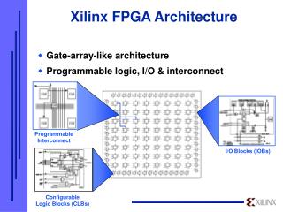
Overview of Xilinx FPGA Architecture I/O Blocks (IOBs) Programmable Interconnect Configurable Logic Blocks (CLBs) Tristate Buffers Global Resources EE514
LUT FF CLB Resources • Basic resource unit is the Logic Cell • 1 CLB contains 2 - 4 Logic Cells, depending on device family • Logic Cell = 4-input Look-Up Table (LUT) + D Flip-flop • LUT capacity limited by number of inputs, not complexity of function • LUTs can be used as ROM or synchronous RAM • Flip-flop can be configured as a transparent latch in Virtex and Spartan-II EE514
Why Synchronous Design? • Synchronous circuits are more reliable • Events are triggered by clock edges which occur at well-defined intervals • Outputs from one logic stage have a full clock cycle to propagate to the next stage • Skew between data arrival times is tolerated within the same clock period • Asynchronous circuits are less reliable • A delay may need to be a specific amount (e.g. 12ns) • Multiple delays may need to hold a specific relationship (e.g. DATA arrives 5ns before SELECT) EE514
Asynchronous Design:Case Studies • What did Xilinx change in their FPGAs? • SRAM process improvements and geometry shrinks increase speed • Normal variations between wafer lots • My Lab was working, but I re-routed my FPGA and now my design fails. What is happening? • Logic placement has changed, which affects internal routing delays • My Lab passes a timing simulation test but fails in circuit. Is the timing simulation accurate? YES • Timing simulation uses worst-case delays • Actual operating conditions are usually better EE514
Design Tips • Reduce clock skew • Clock dividers • Avoid glitches on clocks and asynchronous set/reset signals • The Global Set/Reset network • Select a state machine encoding scheme • Access carry logic • Build efficient counters EE514
INPUT Q_B Q_C D D D Q_A CLOCK 7.5 A B C 3 cycles Clock Q_A Q_B Q_C 2 cycles A & C Clock B Clock 3.0 3.1 3.0 3.3 3.1 Q_A Clock skewed version Expected operation Q_B Q_C Clock Skew • This shift register will not work because of clock skew! EE514
Use Global Buffers to Reduce Clock Skew • Global buffers are connected to dedicated routing • This routing network is balanced to minimize skew • All Xilinx FPGAs have global buffers • XC4000E/L and Spartan have 4 BUFGPs and 4 BUFGSs • XC4000EX/XL/XV and SpartanXL have 8 BUFGLSs • Virtex and Spartan-II have 4 BUFGs • You can always use a BUFG symbol and the software will choose an appropriate buffer type • All major synthesis tools can infer global buffers onto clock signals that come from off-chip
D Q CLK2 D Q BUFG BUFG CLK1 Traditional Clock Divider • Introduces clock skew between CLK1 and CLK2 • Uses an extra BUFG to reduce skew on CLK2 • Design contains 2 clock signals EE514
D Q CLK2_CE CE D Q CLK1 BUFG Recommended Clock Divider • No clock skew between flip-flops • Design now contains only 1 clock EE514
MSB 0111 1000 transition can become 0111 1111 1000 due to faster MSB MSB shorter routing FF LSB glitch may occur here Binary Counter Avoid Clock Glitches • Because flip-flops in today’s FPGAs are very fast, they can respond to very narrow clock pulses • Never source a clock signal from combinatorial logic • Also known as “gating the clock” EE514
D INPUT Q3 D Q2 Q CE Q1 Q0 FF CLOCK Counter Avoid Clock Glitches • This circuit creates the same function, but without glitches on the clock EE514
INPUT Q D Asynchronous Reset FF Binary Counter CLR RESET Q[x] Q[0] CLOCK Avoid Set/Reset Glitches • Glitches on asynchronous Set/Reset inputs can lead to incorrect circuit behavior EE514
INPUT Q D Synchronous Reset FF Counter R RESET Q[x] Q[0] CLOCK Avoid Set/Reset Glitches • Convert to synchronous set/reset when possible EE514
Global Set/Reset (GSR) • Automatically connects to all CLB and IOB flip-flops via a dedicated routing network • Saves general routing resources for your design • Access GSR by instantiating the STARTUP primitive • Some synthesis tools can infer GSR • Use GSR when you have a chip-wide asynchronous reset signal and are targeting Spartan or XC4000 devices Q1 GSR Q2 GTS Q3 STARTUP Q4 CLK DoneIn
State Machine Encoding • Two main FSM encoding schemes • Full Encoding: minimum number of flip-flops possible • Example: S1 = 00, S2 = 01, S3 = 10, S4=11 • State assignments may follow a simple binary count sequence (Binary Encoding), or a more complex sequence • One-Hot Encoding: one flip-flop for each state • S1 = 0001, S2 = 0010, S3 = 0100, S4 = 1000 EE514
Encoding Considerations • Full encoding • Fewer flip-flops • Few or no possible illegal states • Uses logic to decode the present state • Can create multiple logic levels, decreasing performance • Careful state assignment may simplify decoding • One-Hot encoding • More flip-flops • Many possible illegal states • No logic required to decode current state • Can simplify next-state logic, increasing performance
RAM Contents RAM Address = State Machine Inputs + Current State State Machine Outputs Next State FPGAs and State Machines • For higher performance, use One-Hot Encoding • FPGAs have lots of flip-flops • Use Block SelectRAM to implement fast, complex, fully encoded state machines • Initialize the RAM with a “microcode” program
Accessing Carry Logic • All major synthesis tools can infer carry logic for arithmetic functions • Addition (SUM <= A + B) • Subtraction (DIFF <= A - B) • Comparators (if A < B then…) • Counters (count <= count +1) • LogiBLOX or the CORE Generator System • Accumulators • Adder/subtracters • Comparators • Counters (Binary style only) EE514
Accessing Carry Logic • Carry-based library macros • ACCx accumulators • ADDx adders • ADSUx adder/subtracters • CCxcounters • COMPMCx magnitude comparators
10-bit SR Large Dense Counter with Slower Carry CE Fast Small Counter TC Q0 Q6 Q9 Efficient Counters • Prescaler for ultra-fast, non-loadable binary counters • LSBs toggle quickly • Remaining bits have more time to settle • Linear feedback shift register for speed • When terminal count is all that is needed • When any regular sequence is acceptable (e.g. FIFO address counter) EE514
Summary for FPGA Design Techniques • Proper use of hierarchy aids design readability and debug • Synchronous designs are more reliable than asynchronous designs • FPGA design tips • Global clock buffers eliminate skew • Avoid glitches on clocks and asynchronous set/resets • FSM encoding scheme can affect design performance • Increase performance of arithmetic functions by using carry logic • Consider different counter styles to meet your design needs