Memory Devices, Circuits, and Subsystem Design
620 likes | 850 Views
Chapter 9. Memory Devices, Circuits, and Subsystem Design. Chapter nine explore the following topics:. PROGRAM AND DATA STORAGE MEMORY. PROGRAM AND DATA STORAGE MEMORY.

Memory Devices, Circuits, and Subsystem Design
E N D
Presentation Transcript
Chapter 9 Memory Devices, Circuits, and Subsystem Design
PROGRAM AND DATA STORAGE MEMORY Secondary storage memory is used for storage of data, information, and programs that are not in use. This part of the memory unit can be slow speed, but lt require very large storage capacity. Primary storage memory is used for working information, such as the instructions of the program currently being run and data that it is processing. This section normally requires high-speed operation but does not normally require very large storage capacity. Primary storage memory is further partitioned into program storage memory and data storage memory. The much larger part of the program storage memory in a PC is built with dynamic random access read/write memory devices ( DRAMS). They may be either mounted on the main processor board or on an add-in memory module or board. Its purpose is to store programs that are to be executed, but in this case they are loaded into memory only when needed. Information that frequently changes is stored in the data storage part of the microcomputer‘s memory subsystem.
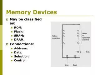
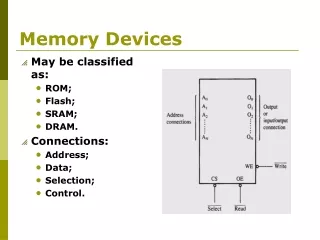
Read Only Memory • Three types of ROM devices are in wide use: • Mask-programmable readonly memory (ROM). • One-time-programmable read-only memory (PROM). • Erasable programmable read-only memory (EPROM). CE: Chip Enable OE: Output Enable
Expanding EPROM Word Length and Word Capacity (a) Expanding word length (b) Expanding word capacity
RANDOM ACCESS READ/WRITE MEMORIES • RAM is similar to ROM in that its storage location can be accessed in a random order, but it is different from ROM in two important ways: • First. RAM can be used to save data by writing to it, and then reading back for additional processing. • Second. RAM is volatile that is, if power is removed from RAM, the stored data are lost Static and Dynamic RAMs • For a Static RAM (SRAM) , data once entered, remain valid as long as the power supply is not turned off. • To retain data in a Dynamic RAM (DRAM), we must both keep the power supply turned on and periodically restore the data in each storage location. • This added requirements necessary because the storage elements in a DRAM are capacitive nodes. If the storage nodes are not recharged within a specific interval of time, data are lost. This recharging process is known as refreshing the DRAM.
A Static RAM System 16K x 16-bit SRAM circuit.
The waveforms for a typical write cycle. • All critical timing is referenced to the point at which the address becomes valid. • The minimum duration of the write cycle is identified as twc. This is the 100-ns write cycle time of the 4364-10. The address must remain stable for this complete interval of time. • CE1 and CE2, become active and must remain active until the end of the write cycle. • The duration of these pulses are identified as CE1 to end of write time (tCW1), and CE2 to end of write time (tCW2). • They begin at any time after the occurrence of the address but before the leading edge of WE. • The minimum value for both of these times is 80 ns. • WE is shown not to occur until the interval tAS elapses. This is the address-setup time and represents the minimum amount of time the address inputs must be stable before WE can be switched to logic 0. • For the 4364 this parameter is equal to 0 ns. • The width of the write enable pulse is identified as twp, and its minimum value equal 60 ns.
Cont. • Data applied to the DIN data inputs are written into the device synchronous with the trailing edge of WE. • The data must be valid for an interval equal to tDW before this edge. • This interval called data valid to end of write, has a minimum value of 40 ns for the 4364-10. • Data remains valid for an interval of time equal to tDH after this edge. • This data hold time similar to address-setup time, equals 0 ns for the 4364. • A short recovery period takes place after WE returns to logic 1 before the write cycle is complete. • This interval is identified as tWR in the waveforms, and its minimum value equals 5 ns.
Standard Dynamic RAM ICs Dynamic RAMS are available in higher densities than static RAMS • Some other benefits of using DRAMS over SRAMS are that: • They cost less, consume less power. • Their 16-and 18-pin packages take up less space. • For these reasons DRAMS are normally used in applications that require a large amount of memory. For example most systems that support at least 1Mbyte of data memory are designed using DRAMS.
DIMMSDRAM with 168-pin MDDR is an acronym that some enterprises use forMobile DDRSDRAM, a type of memory used in some portable electronic devices, likemobile phones, handhelds, anddigital audio players. Through techniques including reduced voltage supply and advanced refresh options, Mobile DDRcan achieve greater power efficiency.
A Dynamic RAM System 64K x l6-bit DRAM circuit
PARITY, The PARITY BIT, AND PARITY-CHECKER/ GENERATOR CIRCUIT In microcomputer systems, the data exchanges that lake place between the MPU and the memory must be done without error. However, problems such as noise, transient signals, or even bad memory bits can produce errors in the transfer of data and instructions. To improve the reliability of information transfer between the MPU and memory, a parity bit can be added to each byte of data. To implement! data transfers with parity, a parity checker/generator circuit is required.
PARITY-CHECKER/ GENERATOR CIRCUIT If the parity is correct, the parity-checker/generator signals this fact to the MPU by making the parity error (PE’) output inactive logic 1. This signal is normally sent to the MPU to identify whether or not a memory parity error has occurred. If an odd number of bits are found to be logic 1. a parity error has been detected and PE’ is set to 0 to tell the MPU of the error condition. Once alerted to the error. the MPU can do any one of a number of things under software control to recover. For instance, it could simply repeat the memory-read cycle to see if it takes place correctly the next time.
FLASH M EMORY FLASH memory devices are similar to EPROMS in many ways, but are different in several very important ways The key difference between a FLASH memory and an EPROM is that its memory cells are erased electrically, instead of by exposure to ultraviolet light. That is, the storage array of a FLASH memory can be both electrically erased and reprogrammed with new data. Unlike RAMS, they are not byte erasable and writeable. when an erase operation is performed on a FLASH memory, either the complete memory array or a large block of storage locations, not just one byte, is erased. Even through FLASH memories are writeable, like EPROMS they find their widest use in microcomputer systems for storage of firmware. However their limited erase/rewrite capability enables their use in applications where data must be rewritten, though not frequently. Some examples: implementation of a nonvolatile writeable lookup table, in-system programming for code updates, and solid state drives. An example of the use of flash memory as a lookup table is the storage of a directory of phone numbers in a cellular phone.
Bulk-Erase, Boot Block, and FlashFile FLASH Memories FL ASH memory devices are available with several different memory array architecture . These architectures related to how the device is organized for the purpose of erasing. In a Bulk-Erase device, the complete storage array is arranged as a single block. Whenever an erase operation is performed, the contents of all storage locations are cleared. The blocks at a boot block device are asymmetrical in size. Boot Block: intended for storage of the boot code for the system. Parameter blocks: storage of certain system parameters, for instance, a system configuration table or lookup table. Main blocks: storage of the firmware code, FlashFile architecture FLASH memory devices: memory array is organized into equal-sized blocks. For this reason it is said to be symmetrically blocked. This type of organization is used in the design of high-density devices which are used in applications that require a large amount of code or data to be stored (e.9 , a FLASH memory drive).
WAIT-STATE CIRCUITRY wait-state generator
WAIT-STATE CIRCUITRY Depending on the access time of the memory devices used and the clock rate of the MPU, a number of wait states may need to be inserted into external memory read and write operations. In the study of 8088/8086 bus cycles we found that the memory subsystem signals the MPU whether or not wait states are needed in a bus cycle with the logic level applied to its READY input. The READY output is returned directly to the READY input of the MPU. Logic 1 at this output tells the MPU that the current read/write operation is to be completed. Logic 0 means that the memory bus cycle must be extended by inserting wait states.
WAIT-STATE CIRCUITRY The circuit represents operation with two wait states
8088/8086 MICROCOMPUTER SYSTEM MEMORY CIRCUITRY Minimum mode 8088 system memory interface