Combiner functionalities
Combiner functionalities. BEAM PERMIT CONTROL Beam dump line survey from the Threshold comparators (TC) through P0 daisy chain lines. TESTS Related to the Beam Interlock Related to the HV (use of VME DBT) ANALOG GENERATION Control of the HV with 0-10V Modulation of the HV

Combiner functionalities
E N D
Presentation Transcript
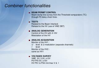
Combiner functionalities • BEAM PERMIT CONTROLBeam dump line survey from the Threshold comparators (TC) through P0 daisy chain lines. • TESTSRelated to the Beam InterlockRelated to the HV (use of VME DBT) • ANALOG GENERATIONControl of the HV with 0-10VModulation of the HV • ANALOG ACQUISITIONMonitor of the HV1 :U level & U modulation (separate channels)I level Monitor of the HV2 :same as HV1 • VOLTAGES SURVEYVME 5V, 3.3V, ±12VP0 FPS 5V, ±15VHV PS1 & PS2 min/max V & I
Combiner functionalities : Tests • BIL Beam Inhibition Lines(test of the lines between DAB and Combiner). • Inhibition test for the LBIS(LHC Beam Interlock System - Combiner). • HTAT step of the HT. Step of the HT activating a TEST_CFC on the tunnel card. • HTLF Low frequency modulation of the HTModulation of the high tension power supplies an analysis of the running sums. • HT monitoringContinuous check of the voltage and current for the 2 power supplies. • VME Supplies monitoringContinuous check of the 5V, 3.3V and ±12V. • P0 Floating SuppliesContinuous check of the 5V and ±15V.
Combiner functionalities Beam permit related parts BLETC Beam Dump (M & UM) Beam permitdecision unit P0 Connector Power Supplies Comparators Logic Beam Energy (Serial) Auto-testBloc CTRV Beam Energy (Serial) BLECS (up) Post-mortem Beam permit P2 Connector Beam info BLECS (down) or BIS FPGA Beam permit Comparators HV1 12 lines HV2 VME PS 4x P0 PS 3x
Combiner functionalities Beam permit related parts Beam Permit from TC (M) Beam Permitdecision unit Beam Permit to BIS (MA) Beam Permit from TC (U) Beam Permit to BIS (MB) Beam Permit from BLECS (MA) Beam Permit to BIS (UA) Beam Permit from BLECS (MB) Beam Permit to BIS (UB) Beam Permit from BLECS (UA) Post-mortem or Login Beam Permit from BLECS (UB) Beam Energy Failure Auto-Test Failure Inhibits Time Stamps (orbit counter) FPGA Synchro & Clocks from BOBR
Combiner functionalities Registers structure VME VME MUX Register DEBUG DEBUG Other source Application External memory Interface DEBUG VME Register
Combiner functionalities Auto-test overview BLETC BLECS“Combiner” Control0-6.8V VME HV(Vin*300) Real excitation signal SURFACE Optical Link BLECF TUNNEL Current HV 0-2000V BLM chamber
Combiner functionalities Auto-test related parts BLETC Control Registers VME SLAVE FPGA P1 & P2 Con. VME MASTER SRAMControl Access SRAM HV1 DAC SPI Auto-testlogic P2 Connector Beam permitdecision unit ADC HV2 SPI I2C Phase & Gaintracking SignalGeneration NVMemory Potentiometers LEDS
Combiner functionalities Auto-test related parts Real ExcitationSignal NVMemory 2-PORT RAM 4x128x32bits Phase & Gaintracking Thresholds Decision Unit TC (16 max) 2-PORT RAM 4x128x32bits Phase & Gaintracking Thresholds Decision Unit VME MASTER UNIT 1 TC 2-PORT RAM 4x128x32bits Phase & Gaintracking Thresholds Decision Unit 2-PORT RAM 4x128x32bits Phase & Gaintracking Thresholds Decision Unit Excitation Signal frequency 0.3Hz Sample per period 128 Number of period 3 Number of channel in parallel 16 (1 TC) Total time for one create 3*1/0.3Hz*16TC = 160s The combiner need to access the VME bus every 1/.3Hz*128 = 26ms
Combiner functionalities BEAM PERMIT CONTROL Task : Receive the Beam Dump request From the Threshold Comparators (TC) and transmit it to the Beam Interlock System (BIS) +5V TC N (DAB) COMB 1 Beam permit Comb – Comb Comb - BIS Beam dump TC - TC TC - Comb TC N (DAB) COMB 2 +3.3V TC 1 (DAB) TC 2 (DAB) TC N (DAB) BIS COMBINER 3
Combiner functionalities BEAM PERMIT CONTROL • Beam dump lines : • From TC to TC • From TC to the Combiner Lines from TC board N-1 Lines to TC board N+1 or to the Combiner Lines from FPGA Needs frequency >1MHz to retrig the One shot
Combiner functionalities BEAM PERMIT CONTROL • Beam permit lines : • From Combiner to Combiner • From Combiner to Beam interlock (BIS) Lines to Combiner board, next create or to the BIS Lines from Combiner board N-1 Lines from FPGA of the combiner representing all other sources of beam dump: Voltage survey, non satisfying test, etc
Combiner functionalities BEAM PERMIT CONTROL Beam permit lines Combiner to BIS
Combiner functionalities BEAM PERMIT CONTROL PCB Implementation Beam Dump lines from the TC Beam permit lines from previous combiner to next combiner or BIS
Combiner functionalities ANALOG GENERATION The high voltage power supplies for the ionization chambers are controlled by analog signals 0-10V. There is an analog sum done between the 2 outputs of the DAC, the modulation signal is attenuated with a potentiometer digitally controlled. To the HV supply0-10V Voltage Control Serial Peripheral Interface From the FPGA 16 bits DAC8532 Analog SUM Offset Modulation Pot digitally Controlled (8 bits steps) Inter Integrated Circuit (I2C) bus to the FPGA
Combiner functionalities ANALOG GENERATION SCHEMATIC
Combiner functionalities ANALOG ACQUISITION The high voltage power supplies have monitor analog output to view the voltage and current levels, there is 1 channel for the current and 2 channels of digitalization for the voltage (offset and low frequency modulation ADC Buffer LP Filter From the HV supply0-10V Voltage Monitor Serial Peripheral Interface To the FPGA Instrumentation amplifier Inter Integrated Circuit (I2C) bus to the FPGA Offset compensation +15V GAIN Digital pot. Digital pot. +0V From the HV supply0-10V Current Monitor Buffer LP Filter
Combiner functionalities ANALOG ACQUISITION
Combiner functionalities ANALOG DIGITAL CONVERSIONS PCB Implementation Analog generation for the 2 HV PS Digitalization of the information coming from the 2 HV power supplies RC filter close to the connector to cut the eventual high frequencies induced by the digital components
Combiner functionalities VOLTAGES SURVEY HV SUPPLY There is a second survey of the HV power supplies level with comparators with fixed level (to be determined) Lower and higher limit for the voltage and lower and higher limit for the current. Resistor calculated for the schematic shown U min = 1333V U max = 1666V
Combiner functionalities VOLTAGES SURVEY VME & P0 floating PS VME POWER SUPPLIES:5V, 3.3V, ±12VP0 FLOTING POWER SUPPLIES:5V, ±15V
Combiner functionalities VOLTAGES SURVEY 1) HV SUPPLIES 2) VME & P0 floating PS Survey VME PS Survey P0 floating PS Survey HV PS
Combiner functionalities Commune lines between crates • Task : • Synchronize the beginning of the auto-test because it’s only the COMB 3 which control the HV PS for all the 3 creates. • Other task ? COMB 1 COMB 2 Open drain lines COMB 3 Comb 1release line Comb 2release line Comb 2release line Begin test Wait state
Combiner prototypes and production test • FIRST VERSION PROTOTYPEAs fast as possible on production with test points as much as possible on the analog lines.=> Functional test of these prototypes. • EVALUATIONmodification of the JTAG test developed for the DAB (60% coverage on the DAB) and/or use of a test board & JTAG (90% coverage on the DAB). Visual & functional test for the analog parts. • NEW PROTOTYPES • TEST DEVELOPMENT • PRODUCTION