Download
1 / 15
150 likes | 161 Views
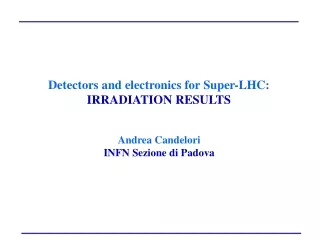
This article presents the irradiation results of detectors and electronics for the Super-LHC. The experiments were performed by the SMART Collaboration and the Department of Information Engineering at the University of Padova. Measurements were conducted on various types of detectors that were irradiated with neutrons and protons at different fluences. The effects of irradiation and annealing on the detectors' performance were analyzed. Additionally, the impact of proton irradiation on the electronics was also studied.

E N D
Detectors and electronics for Super-LHC: IRRADIATION RESULTS Andrea Candelori INFN Sezione di Padova
OUTLINE • The presented results are from experiments performed by: • SMART Collaboration (Bari, Firenze, Pisa, Padova, Perugia, Trieste, Trento) • Department of Information Engineering (DEI), University of Padova • Measurements are in progress … 1) Nuclear reactor irradiation in Lubiana: -MCZ n-type detectors (SMART) -Epitaxial n-type detectors (SMART) 2) 24 GeV proton irradiation at CERN: -Epitaxialn-type detectors (SMART) -FZ thinned n-type detectors (SMART) - 0.13 mCMOS technology (DEI)
DETECTORS -MCZ detectors Substrate: MCZ, n-type, 300 m thick, =0.6 k×cm, from Okmetic Detector processing: IRST -Epitaxial detectors Epitaxial layer: n-type, 50 m thick, = 50 cm, grown by ITME on CZ substrate Detector processing: IRST -FZ thinned detectors Substrate: FZ, n-type, 300 m thick,=6 k·cm Thinning: down to 50-100 m by Tetra Methyl Ammonium Hydroxide (TMAH) etching from backside: IRST Detector processing: IRST
MCZ n-type 300 m thick detectors: neutron irradiation Measurements after irradiation and before annealing The minimum of Vdep is reached at 1-1.5×10¹⁴ n/cm2. Vdep is 650 at 1015 n/cm2.
Measurements after irradiation and before annealing Epitaxial n-type 50 m thick detectors: neutron irradiation The minimum of Vdep40-50 V is reached at 2-4×10¹⁵ n/cm2. Vdep< Vdep,0 at 8×10¹⁵ n/cm2.
120 100 F (n/cm2) 1×10¹⁵ 80 2×10¹⁵ (V) 3×10¹⁵ 60 dep 4×10¹⁵ V 6×10¹⁵ 40 8×10¹⁵ 20 0 1 10 100 ° Annealing time at 80 C (min) Epitaxial n-type 50 m thick detectors: neutron irradiation Vdep decreases for annealing times at 80 C higher than 8 minutes. If this effect is due to deep acceptor generation, devices are not type inverted.
0.35 0.30 after irradiation ) 3 4 min at 80C 0.25 8 min at 80C C (A/cm 16 min at 80C 32 min at 80C 0.20 ° 0.15 scaled to 20 0.10 D J 0.05 0.00 0 1 2 3 4 5 6 7 8 9 15 2 Fluence (10 1 MeV equivalent neutrons/cm ) Epitaxial n-type 50 m thick detectors: neutron irradiation JD increases linearly with fluence. JD decreases with annealing time at 80 C.
Epitaxial n-type 50 m thick detectors: neutron irradiation 0.35 0.30 ) 3 0.25 C (A/cm F (n/cm2) 0.20 ° 8×10¹⁵ 6×10¹⁵ 0.15 scaled to 20 4×10¹⁵ 0.10 3×10¹⁵ D 2×10¹⁵ J 0.05 1×10¹⁵ 0.00 1 10 100 ° Annealing time at 80 C (min) JD decreases with annealing time at 80 C.
Epitaxial n-type 50 m thick detectors: proton irradiation Measurements after irradiation and before annealing neutrons The minimum of Vdep for protons (90-100 V) is higher than for neutrons (40-50 V). Vdep> Vdep,0 at 1016 p/cm2. The radiation effects induced by neutrons and protons are different.
300 250 F (p/cm2) 200 Before irr. 2.2×10¹⁵ (V) 150 4.0×10¹⁵ dep V 8.3×10¹⁵ 100 10.1×10¹⁶ 50 0 1 10 100 1000 10000 ° Annealing time at 80 C (min) Epitaxial n-type 50 m thick detectors: proton irradiation • Vdep decreases for annealing times at 80 C higher than 8 minutes. • If this effect is due to deep acceptor generation, devices are before SCSI after irradiation: • for devices irradiated at low fluences Vdep ↑, ↓: no SCSI during long-term annealing; • for devices irradiated at high fluences Vdep↑, ↓, ↑: SCSI during long-term annealing.
FZ thinned n-type detectors: proton irradiation 300 Measurements after irradiation and before annealing 100 m 200 50 m (V) 50 m dep V 100 0 0 2 4 6 8 10 12 15 2 Fluence (10 24 GeV protons/cm ) Device thinning limits the Vdep increase after irradiation: -Vdep290 V for 100 m thick detectors at 8×10¹⁵ p/cm2 -Vdep70 V for 50 m thick detectors at 1016 p/cm2
FZ thinned n-type detectors: proton irradiation 0.30 Measurements after irradiation and before annealing ) 0.25 3 C (A/cm 100 m 0.20 50 m ° 0.15 50 m scaled to 20 0.10 D J 0.05 0.00 0 2 4 6 8 10 12 15 2 Fluence (10 24 GeV protons/cm ) JD linearly increases with fluence, independently on the thickness. (some data dispersion is present)
DETECTORS: future activity CERN, 24 GeV protons, May 2004 (n-type materials) Lubiana, nuclear reactor neutrons, December 2004 (n- and p-type materials)
ELECTRONICS -Electronics for LHC (10 Mrad(Si) and 1015 fast hadrons/cm2): 0.25 m CMOStechnology fromIBM; 5.5 nm oxide thickness; radiation hardened by design: enclosed geometry transistors. The 0.25 m CMOS technology will not be any more available for Super-LHC -Electronics for Super-LHC (100 Mrad(Si) and 1016 fast hadrons/cm2): following the scaling down of the commercial CMOS technologies? 0.13 m minimum channel length; 2.5 nm oxide thickness; no radiation hardened by process; no radiation hardened by design (i.e., no enclosed geometry).
0.13 m CMOS technology: proton irradiation p-channel MOSFET n-channel MOSFET gM peak decrease 15% gM peak shift negligible gM peak decrease higher than in n-MOSFET gM peak shift of 200 mV