Download
1 / 2
20 likes | 147 Views
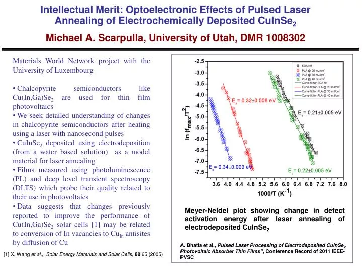
Intellectual Merit: Optoelectronic Effects of Pulsed Laser Annealing of Electrochemically Deposited CuInSe 2 Michael A. Scarpulla , University of Utah, DMR 1008302. Materials World Network project with the University of Luxembourg

E N D
Intellectual Merit: Optoelectronic Effects of Pulsed Laser Annealing of Electrochemically Deposited CuInSe2Michael A. Scarpulla, University of Utah, DMR 1008302 • Materials World Network project with the University of Luxembourg • Chalcopyrite semiconductors like Cu(In,Ga)Se2 are used for thin film photovoltaics • We seek detailed understanding of changes in chalcopyrite semiconductors after heating using a laser with nanosecond pulses • CuInSe2 deposited using electrodeposition (from a water based solution) as a model material for laser annealing • Films measured using photoluminescence (PL) and deep level transient spectroscopy (DLTS) which probe their quality related to their use in photovoltaics • Data suggests that changes previously reported to improve the performance of Cu(In,Ga)Se2 solar cells [1] may be related to conversion of In vacancies to CuIn antisites by diffusion of Cu Meyer-Neldel plot showing change in defect activation energy after laser annealing of electrodeposited CuInSe2 A. Bhatia et al., Pulsed Laser Processing of Electrodeposited CuInSe2 Photovoltaic Absorber Thin Films”, Conference Record of 2011 IEEE-PVSC • [1] X. Wang et al., Solar Energy Materials and Solar Cells, 88 65 (2005)
Broader Impacts: Optoelectronic Effects of Pulsed Laser Annealing of Electrochemically Deposited CuInSe2Michael A. Scarpulla, University of Utah, DMR 1008302 Ashish Bhatia learned electrochemical deposition of CuInSe2 during his week-long stay at U Luxembourg, Nov. 2010. This project is in collaboration with Dr. Phillip Dale at the University of Luxembourg, who has expertise in electrochemical deposition of semiconductors for photovoltaics. The team meets bi-weekly via Skype. After the full-team kickoff visit in Luxembourg, U of Utah PhD student Ashish Bhatia stayed to learn electrodeposition of CuInSe2 as well as multiple characterization techniques. Dr. Dale visited U of Utah in April 2011 in conjunction with MRS Spring. Currently 6 undergraduates from both Materials Science and Electrical Engineering are working on this project at the U of Utah. A collaborative reference website for earth-abundant photovoltaics is being constructed. Full MWN team in Luxembourg, Nov. 2010 (H. Meadows, A. Bhatia, P. Dale, & M. Scarpulla) Undergraduate Mitchell Hymas working with the pulsed Nd:YAG laser at U Utah