Download
1 / 2
20 likes | 206 Views
Materials World Network Fumio S. Ohuchi, University of Washington, DMR 0710641. Phase Change Materials for Nanoelectronics. • Overall Project: US-Japan Partnership focused on nanoscale understanding of phase transformation for semiconductor applications.

E N D
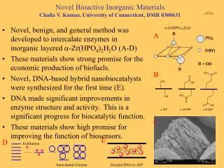
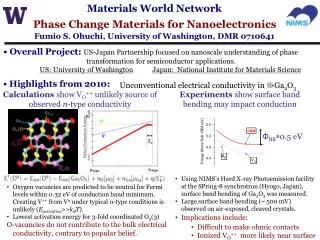
Materials World NetworkFumio S. Ohuchi, University of Washington, DMR 0710641 Phase Change Materials for Nanoelectronics • Overall Project:US-Japan Partnership focused on nanoscale understanding of phase transformation for semiconductor applications. US: University of WashingtonJapan: National Institute for Materials Science •Highlights from 2010: Unconventional electrical conductivity in β-Ga2O3 Calculations show VO++ unlikely source of observed n-type conductivity Experiments show surface band bending may impact conduction ΦBB≅0.5 eV • Oxygen vacancies are predicted to be neutral for Fermi levels within 0.32 eV of conduction band minimum. Creating V++ from V0 under typical n-type conditions is unlikely (Eactivation>>kBT). • Lowest activation energy for 3-fold coordinated O3(3) O-vacancies do not contribute to the bulk electrical conductivity, contrary to popular belief. • Using NIMS’s Hard X-ray Photoemission facility at the SPring-8 synchrotron (Hyogo, Japan), surface band bending of Ga2O3 was measured. • Large surface band bending (~ 500 mV) observed on air-exposed, cleaved crystals. • Implications include: • Difficult to make ohmic contacts • Ionized VO++ more likely near surface
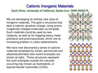
Broader Impact of the Project Fumio S. Ohuchi, University of Washington, DMR 0710641 This project is a multi-national collaboration involving three departments (Materials Sci. & Eng., Physics, and Elec. Eng.) at the University of Washington in Seattle, WA and two groups from National Institute for Materials Science (Crystal Growth group, and SPring-8 group) in Japan. By doing experiments in foreign research facilities, students gain excellent diversity training by experiencing being in the minority first hand. Also, students are trained in establishing collaborations abroad and at home. Left: Tracy Lovejoy (left), a UW graduate student, experiences being a minority first hand during a long collaboration at SPring-8 synchrotron facility. Professor Fumio Ohuchi (right) offers advice with SPring-8 in the background. Right: Patrick Shamberger, a UW graduate student, enjoyed working with Dr. Yoshiyuki Yamashita, a beam line scientist. MWN program helped to grow NIMS’s Overseas Operation Office (O3) Further development of UW-NIMS joint research projects Student exchange through coordinated UW-NIMS graduate program Development of UW-NIMS administrative infrastructure Establishment of joint venture company Held joint UW-NIMS research forum Since its inception 2.0 years ago, NIMS has invested >$450K to operate this overseas office. This office also fostered visits of the UW-faculty to NIMS through the MWN program. Forum reception at the House of Japanese Consul General