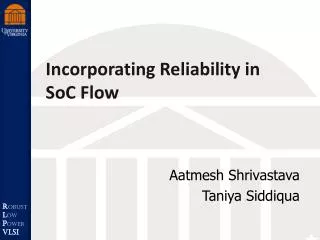
Incorporating Reliability in SoC Flow
270 likes | 452 Views
Incorporating Reliability in SoC Flow. Aatmesh Shrivastava Taniya Siddiqua. Motivation. Intel Nehalem™. IBM POWER7™. AMD Phenom™. Abstraction of Reliable Hardware. Moore’s Law. Silicon Reliability. NBTI. PBTI. EM. TDDB. Implement DFR to Ensure Long-term Reliability.

Incorporating Reliability in SoC Flow
E N D
Presentation Transcript
Incorporating Reliability in SoC Flow Aatmesh Shrivastava Taniya Siddiqua
Motivation Intel Nehalem™ IBM POWER7™ AMD Phenom™ Abstraction of Reliable Hardware Moore’s Law
Silicon Reliability NBTI PBTI EM TDDB Implement DFR to Ensure Long-term Reliability
Negative Bias Temperature Instability (NBTI) Negative bias No bias ‘1’ ‘1’ Interface traps Recovery phase ‘1’ ‘0’ Increases Vt and circuit delay Causes processor failure Restores Vt Improves delay
Goals Develop reliability spice models from literature. Develop methodology to assess the reliability of the circuit. Obtain the critical paths and characterize it for worst case.
Top-level Flow TransistorModel RTL Design Generate Netlist Std. Cell Degradation Timing Analysis F(t,α,vdd,T,l) Model Critical Path Reliability assesment Obtaining WC Performance
Transistor Reliability Model D G S • Modeling component • VDD • fan_out • Temp • Year • Activity VGS (VDD) VDS (VDD, fan_out) Temp (Temp) Time (year, activity)
Transistor Reliability Model From the implemented Model R.Vattikonda DAC 06 By using MOSRA degraded transistor model can be obtained. However, MOSRA never ran properly. We constructed our own device model using PTM from ASU. http://ptm.asu.edu/
Standard Cell Model VDD, Temp and fanout were varied and there delay at time 0 was calculated for a given std. cell. Device degradation at the given VDD, Temp. and fanout was calculated by further varying activity and time. This will result in ΔVth for each particular corner. Using this we can calculate delay degradation for each particular corner. We can use the obtained degraded delay to construct the reliability model for std. cell as a function of 5 variables.
Standard Cell Model ctd. • Delay was obtained for 10 different activities. • 2nd order polynomial is a good approximation. • Which gives us a function to directly map activity to delay. Varying only activity.
Standard Cell Model ctd. • Delay was obtained for 10 different time. • 2nd order polynomial is a good approximation. • Which gives us a function to directly map stress time to delay. Varying only stress time.
Standard Cell Model ctd. • TDG= (a1*t2+b1*t+c1)*(a2*α2+ b2*α+c2) • TDG=a*t2*α2+b*t*α2+c*α2 + d*t2*α+e*t*α+f*α+g*t2 +h*t+k • 9 variables a, b, …k needed to construct the model • By using 9 different points w.r.t activity and time a, b,.. Can be obtained • Matlab can be used to solve this Combining stress time and activity considering everything else being constant
Standard Cell Model ctd. • Maximum Error 0.5% Coefficients were obtained using the explained procedure. Model was constructed
Standard Cell Model • Proceeding this way dependence on other 3 parameters VDD, Temp and fanout can be established. • Advantages of this model • While we are presenting the solution in the context of reliability, the equation with P, T and V can easily be established for any standard cell. • Potential to replace .libs • Having delay or other characteristics in the form of equation can provide great flexibility in terms of library creation and accounting for cross domain analysis, etc, can enable DVFS in SOC flow. • Since VDD, Temp and fanout are more static than others, we kept the model at this level only. • For each combination of VDD, Temp and fanout, the 9 variable matrix was evaluated.
Standard Cell Model Applying the preceding procedure models for each standard cell can be constructed in the similar fashion However similarity in the std. cell architecture can be leveraged. Each standard cell essentially has push-pull structure like inverter, so they are likely to degrade in the similar fashion. To evaluate this we obtained the relative delay of both inverter and other standard cell and compared.
Standard Cell Model • Maximum Error 15% Since the errors were in the range of 15% we chose to use the one model normalized to t=0 delay for each cell. This was done to reduce the effort. For more accuracy model can be constructed for each std. cell.
Top-level Flow TransistorModel RTL Design Generate Netlist Std. Cell Degradation Timing Analysis F(t,α,vdd,T,l) Model Critical Path Reliability assesment Obtaining WC Performance
Obtaining the Critical Path • We use PrimeTime, the Synopsys static timing analysis (STA) tool • PrimeTime performs full-chip static timing analysis with high speed and low memory utilization • Steps: • read a design • link a design to libraries • establish constraints on the design (e.g. electrical loading rules) • specify environmental attributes • perform timing analysis.
PrimeTime Requirements • Verilog description should be either a gate-level database file (.ddc) or a Verilog file generated by Design Compiler (the Synopsys synthesis tool) • Failing to observe this will lead to 0 delay paths when you execute report_timing • Such modules are treated as "black boxes" with no timing arcs, as the system appears to ignore the library cell delays if the modules use position association instead of name association
Design Compiler • read_verilog ./risc_core.v • analyze -library WORK -format verilog {./risc_core.v} • elaborate RISC_CORE -architecture verilog -library DEFAULT • link • check_design • compile -exact_map • write -hierarchy -format verilog -output ./results/RISC_CORE.v
Design Constraints File • # Define a clock for synchronous design (constrains all register to register timing paths) • # Required: Clock source, Clock period. Options: Duty cycle, offset/skew, clock name • create_clock-period 9 [get_portsClk] • # Constrain input and output timing paths • set_input_delay-max 1.5 -clock Clk [all_inputs] • set_output_delay 1 -clock Clk -clock_fall -max [all_outputs] • # To specify the fastest arrival time of the external logic to the input ports: • set_input_delay–min 0.25 –clock –Clk [get_ports A] • # To specify the hold time of the external logic on the output ports of the design: • set_output_delay–min –0.25 –clock Clk [get_ports C] • set_wireload_model “enclosed” • set_operating_conditionsWORST
PrimeTime • set search_path ../ref/models • set link_path “* ../ref/models/saed90nm_type.db” • set link_create_black_boxes false • read_verilog /path_to_your_design/source_file_name • link_design –keep_sub_designs $DESIGN_NAME • check_timing • source ./constraints/constraint_file_name.tcl • report_path_group > reports/${DESIGN_NAME}.path_group • report_timing > reports/${DESIGN_NAME}.timing • report_timing -max_paths 10
Critical Path • Point Incr Path • I_INSTRN_LAT/Crnt_Instrn_1_reg[27]/Q (DFFX1) 0.41 0.41 r • I_ALU/U15/ZN (INVX0) 0.29 0.70 f • I_ALU/U4/ZN (INVX0) 0.44 1.14 r • I_ALU/U516/Q (OR2X1) 0.38 1.52 r • I_ALU/U515/QN (NOR2X0) 0.13 1.66 f • I_ALU/U509/ZN (INVX0) 0.33 1.99 r • I_ALU/U479/QN (NOR3X0) 0.33 2.32 f • I_ALU/r24/U1/Q (XOR2X1) 0.25 2.57 f • I_ALU/r24/U1_0/CO (FADDX1) 0.34 2.91 f • I_ALU/U270/Q (MUX21X1) 0.17 8.60 f • I_ALU/U216/Q (AND2X1) 0.13 8.73 f • I_ALU/U223/Q (MUX41X1) 0.26 8.99 f
Critical path degradation • DFF (0.41)=> INV (0.29)=> INV (0.44)=> • OR2 (0.38)=> NOR2 (0.13)=>INV (0.33)=> • NOR3 (0.33)=> XOR2 (0.25)=> • FADD (0.34)=> FADD (0.34)=> FADD (0.34)=> FADD (0.34)=> • FADD (0.34)=> FADD (0.34)=> FADD (0.34)=> FADD (0.34)=> • FADD (0.34)=> FADD (0.34)=> FADD (0.34)=> FADD (0.34)=> • FADD (0.34)=> FADD (0.34)=> FADD (0.34)=> FADD (0.34)=> • FADD (0.37)=> • XOR2 (0.22)=> MUX21 (0.16)=> MUX21 (0.17)=> AND2 (0.13)=> MUX41 (0.26)=> AO22 (0.17)=>DFF (0.04) The critical path degrades from 9.52ns to 10.35ns after 5 yrs. We obtain this using the flow and model.
Summary • Develop reliability spice models from literature. • MOSRA never ran properly. • We constructed our own device model • Develop methodology to assess the reliability of the circuit. • Obtain the critical paths and characterize it for worst case. • Used PrimeTime Static Timing Analysis