
(a)
E N D
Presentation Transcript
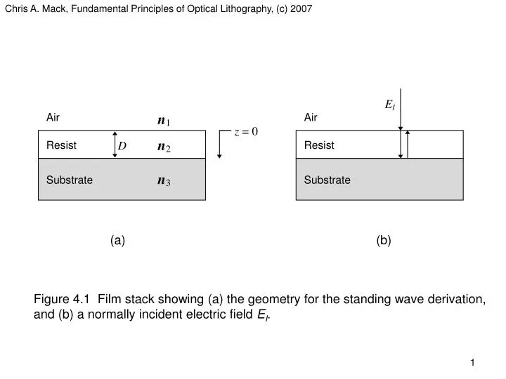
Chris A. Mack, Fundamental Principles of Optical Lithography, (c) 2007 (a) (b) Figure 4.1 Film stack showing (a) the geometry for the standing wave derivation, and (b) a normally incident electric field EI.
Chris A. Mack, Fundamental Principles of Optical Lithography, (c) 2007 Figure 4.2 Standing wave intensity in one micron of photoresist on a silicon substrate for an i-line exposure.
Chris A. Mack, Fundamental Principles of Optical Lithography, (c) 2007 Figure 4.3 Standing wave intensity within a photoresist film at the start of exposure (850nm of resist on 100nm SiO2 on silicon, l = 436nm). Note the impact of the oxide film on the phase of the effective substrate reflectivity, which affects the intensity at the bottom of the resist.
Chris A. Mack, Fundamental Principles of Optical Lithography, (c) 2007 Figure 4.4 Geometry used for describing plane waves and standing waves for oblique incidence.
Chris A. Mack, Fundamental Principles of Optical Lithography, (c) 2007 Figure 4.5 Reflectivity (square of the reflection coefficient) as a function of the angle of incidence showing the difference between s- and p-polarization (n1 = 1.0, n2 = 1.7). Both air and resist layers are assumed to be infinitely thick.
Chris A. Mack, Fundamental Principles of Optical Lithography, (c) 2007 Figure 4.6 Standing wave intensity within a photoresist film (500 nm of resist on silicon, l = 248 nm) as a function of incident angle (s-polarization assumed).
Chris A. Mack, Fundamental Principles of Optical Lithography, (c) 2007 Figure 4.7 Spectral output of a typical high-pressure mercury arc lamp. The illumination spectrum of an i-line or g-line lithographic exposure tool is usually a filtered portion of this lamp spectrum.
Chris A. Mack, Fundamental Principles of Optical Lithography, (c) 2007 Figure 4.8 Standing wave intensity within a photoresist film (1000 nm of resist on silicon), for monochromatic (l = 365 nm) and broadband illumination (350 – 450 nm range of the mercury spectrum).
Chris A. Mack, Fundamental Principles of Optical Lithography, (c) 2007 Figure 4.9 CD swing curve showing a sinusoidal variation in the resist linewidth with resist thickness (i-line exposure of resist on silicon).
Chris A. Mack, Fundamental Principles of Optical Lithography, (c) 2007 Figure 4.10 Eo swing curve showing a sinusoidal variation in the resist dose-to-clear with resist thickness (i-line exposure of resist on silicon).
Chris A. Mack, Fundamental Principles of Optical Lithography, (c) 2007 Figure 4.11 Reflectivity swing curve showing a sinusoidal variation in the resist coated wafer reflectivity with resist thickness (i-line exposure of resist on silicon).
Chris A. Mack, Fundamental Principles of Optical Lithography, (c) 2007 Figure 4.12 Film stack showing (a) geometry for swing curve derivation, and (b) incident, transmitted, and reflected waves (oblique angles are shown for diagrammatical purposes only).
Chris A. Mack, Fundamental Principles of Optical Lithography, (c) 2007 Figure 4.13 The phase and amplitude of a dose-to-clear swing curve are affected by the range of angles striking the resist, which is controlled by the product of the partial coherence and the numerical aperture (sNA) for conventional illumination.
Chris A. Mack, Fundamental Principles of Optical Lithography, (c) 2007 Figure 4.14 Proper balancing of absorption and reflectivities can make the minimum of a swing curve (D = 310 nm) achieve the same CD as the previous swing curve maximum (D = 280 nm).
Chris A. Mack, Fundamental Principles of Optical Lithography, (c) 2007 Figure 4.15 Typical examples of substrate reflectivity versus BARC thickness for different resist/BARC/substrate stacks.
Chris A. Mack, Fundamental Principles of Optical Lithography, (c) 2007 (a) (b) Figure 4.16 Optimum BARC refractive index (real and imaginary parts, n and k) as a function of BARC thickness for normal incidence illumination (resist index = 1.7 + i0.01536 and silicon substrate index = 0.8831 + i2.778) at 193 nm. a) First minimum BARCs, and b) second minimum BARCs.
Chris A. Mack, Fundamental Principles of Optical Lithography, (c) 2007 (a) (b) Figure 4.17 Sensitivity of substrate reflectivity for the optimum first minimum BARCs of Figure 4.16a as a function of a) BARC thickness errors, or b) BARC refractive index errors.
Chris A. Mack, Fundamental Principles of Optical Lithography, (c) 2007 (a) (b) Figure 4.18 Sensitivity of substrate reflectivity for the optimum second minimum BARCs of Figure 4.16b as a function of a) BARC thickness errors, or b) BARC refractive index errors.
Chris A. Mack, Fundamental Principles of Optical Lithography, (c) 2007 (a) (b) Figure 4.19 Optimum BARC parameters to achieve minimum substrate reflectivity as a function of incident angle (angle defined in air, before entering the photoresist) for two different BARC thicknesses (resist index = 1.7 + i0.01536 and silicon substrate index = 0.8831 + i2.778) at 193 nm exposure: a) 20 nm BARC thickness, and b) 40 nm BARC thickness.
Chris A. Mack, Fundamental Principles of Optical Lithography, (c) 2007 Figure 4.20 The best case (minimum) reflectivity (using the BARC parameters shown in Figure 4.19) of the substrate as a function of incident angle for 20nm and 40nm thick BARC films. Note that 60º corresponds to the maximum angle in air allowed for NA = 0.866.
Chris A. Mack, Fundamental Principles of Optical Lithography, (c) 2007 Figure 4.21 An example of the variation of BARC reflectivity as a function of light angle and polarization for two different BARCs. The intensity reflectivity is the square of the electric field reflectivity plotted here, but interference makes the field reflectivity a better measure of the standing wave effects. (Resist index = 1.7 + i0.01536, silicon substrate index = 0.8831 + i2.778, BARC A index = 1.80 + i0.48, BARC A thickness = 30 nm, BARC B index = 1.53 + i0.54, BARC B thickness = 39 nm.)
Chris A. Mack, Fundamental Principles of Optical Lithography, (c) 2007 Figure 4.22 Substrate reflectivity versus BARC thickness over a range of underlying oxide thicknesses (oxide on top of a silicon substrate).
Chris A. Mack, Fundamental Principles of Optical Lithography, (c) 2007 Figure 4.23 CD swing curves (100nm lines with a 280nm pitch are printed with a stepper using annular illumination, with a center sigma given by sNA = 0.54) for two different BARCs with different levels of optimization, as given by the resulting substrate reflectivity R.
Chris A. Mack, Fundamental Principles of Optical Lithography, (c) 2007 Figure 4.24 Example of how resist thickness variations over topography produce linewidth variations due to swing curve effects when a BARC is not used.
Chris A. Mack, Fundamental Principles of Optical Lithography, (c) 2007 Figure 4.25 Reflective notching occurs when nearby topography reflects light obliquely into an adjacent photoresist feature.
Chris A. Mack, Fundamental Principles of Optical Lithography, (c) 2007 Figure 4.26 Imaging of lines and spaces over reflective topography without BARC (left) showing reflective notching, and with BARC (right) showing the reflective notching effectively suppressed (photos courtesy of AZ Photoresist, used with permission).
Chris A. Mack, Fundamental Principles of Optical Lithography, (c) 2007 Figure 4.27 Contrast Enhancement Layer (CEL) bleaching improves the quality of the aerial image transmitted into the photoresist.
Chris A. Mack, Fundamental Principles of Optical Lithography, (c) 2007 Figure 4.28 Variation of the magnitude and phase of the resist/substrate reflection coefficient as a function of silicon nitride thickness for a film stack of resist on nitride on 40 nm of oxide on silicon.
Chris A. Mack, Fundamental Principles of Optical Lithography, (c) 2007 Figure 4.29 Changes in nitride thickness cause a shift in the phase of the resist swing curve, making nitride thickness control as critical as resist thickness control.
Chris A. Mack, Fundamental Principles of Optical Lithography, (c) 2007 Figure 4.30 Nitride thickness also affects the shape of the resist profile, causing resist footing, undercuts, or vertical profiles. Substrate reflectivity (the square of the magnitude of the reflection coefficient) is shown for comparison.
Chris A. Mack, Fundamental Principles of Optical Lithography, (c) 2007 Figure 4.31 Two plane waves with different polarizations will interfere very differently. For transverse electric (TE) polarization (electric field vectors pointing out of the page), the electric fields of the two vectors overlap completely regardless of the angle between the interfering beams.
Chris A. Mack, Fundamental Principles of Optical Lithography, (c) 2007 Figure 4.32 The interference between two TM polarized planes waves produces an image whose contrast and NILS depends on the angle. Since the angle in resist is reduced by refraction, the contrast and NILS of the image in resist is better than the aerial image.
Chris A. Mack, Fundamental Principles of Optical Lithography, (c) 2007 (a) (b) Figure 4.33 Focusing of plane waves arriving at different angles a) in air, and b) in resist, showing that the resist induces spherical aberration.
Chris A. Mack, Fundamental Principles of Optical Lithography, (c) 2007 Figure 4.34 The standing wave amplitude ratio (SWAR) at different positions on the feature for coherent three-beam imaging and s-polarization. For this example of three-beam imaging of 100 nm lines and spaces, ao = 0.5, a1 = 0.3183.
Chris A. Mack, Fundamental Principles of Optical Lithography, (c) 2007 Figure 4.35 Intensity transmitted into layer 2 relative to the incident intensity (solid lines) and the transmittance T (dashed lines) as a function of the angle of incidence for both s and p polarization (n1 = 1.0, n2 = 1.5).