Download
1 / 18
590 likes | 1.27k Views
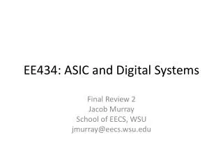
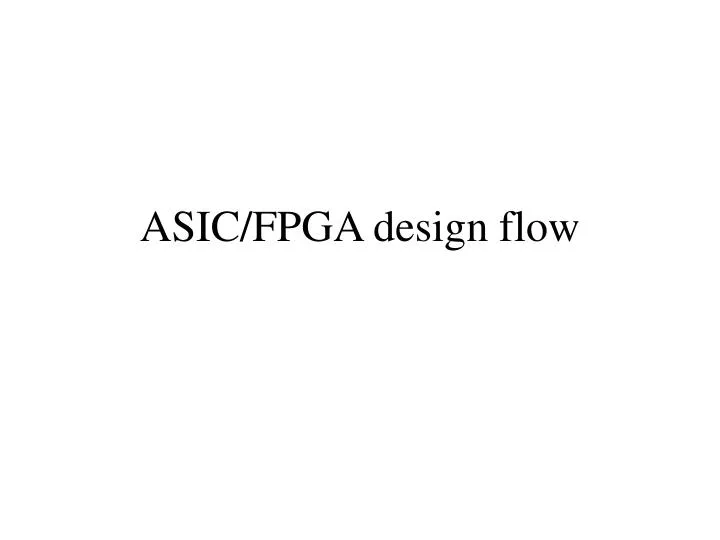
ASIC/FPGA design flow. Design Ideas (Specifications). Detailed (RTL) Design. Functional Simulation. Device Programming. Timing Simulation. Synthesis & Implementation. FPGA CPLD. t pd =22.1ns f max =47.1MHz. FPGA Design Flow. Design Specification.

E N D
Design Ideas (Specifications) Detailed (RTL) Design Functional Simulation Device Programming Timing Simulation Synthesis & Implementation FPGA CPLD tpd=22.1ns fmax=47.1MHz FPGA Design Flow
Design Specification • What are the main design considerations? • Design feasibility? • Performance • power consumption • cost • Design spec? • Written (Document) • Good starting point, but can be misinterpreted by design team • Executable (UML, C/C++, Behavioral VHDL, SystemVerilog) • Harder to understand, less room for misinterpretation • Implementation platform • FPGA/CPLD? • ASIC? • Which FPGA/CPLD vendor? • Which device family? • Development time?
RTL Specification • Determine I/O signals • Standard interface, protocol, custom interface • Partition design into functional blocks • Datapath, Control logic, Memory, etc. • Determine block interfaces • Specify each block separately at RTL • MUXs, counters, adders, flip-flops etc.
Detailed Design • Choose the design entry method • Schematic • Intuitive & easy to debug • Not portable • Poor designer productivity (gates/time) • HDL (Hardware Description Language), e.g. Verilog, VHDL, SystemC • Requires some experience, harder to debug • Descriptive & portable • Easy to modify • Greater productivity • Mixed HDL & schematic • Interpret the specifications • Manage the design hierarchy • Design partitioning • Chip partitioning • Logic partitioning • Use vendor-supplied IP libraries to reduce design time • Create & manage user-created libraries (circuits)
Functional Simulation • Preparation for simulation • Generate simulation patterns • Waveform entry • HDL testbench • Generate simulation netlist • Functional simulation • To verify the functionality of your design only • Simulation results • Waveform display • Text output • Self-checking testbench • Challenge • Sufficient & efficient test patterns
assign z=a&b a z b HDL Synthesis • Synthesis = Translation + Optimization • Translate HDL design files into gate-level netlist • Optimize according to your design constraints • Area constraints • Timing constraints • Power constraints • Main challenges • Learn synthesizable coding style • Use proper design partitioning for synthesis • Specify reasonable design constraints • Use HDL synthesis tools efficiently
a z b FPGA CPLD 01011... Design Implementation • Implementation flow • Netlist merging, flattening, data base building • Design rule checking • Logic optimization • Block mapping & placement • Net routing • Configuration bitstream generation (FPGA only) • Scan flip-flop insertion (ASIC only) • Implementation results • Design error or warnings • Device utilization (FPGA) • Die size (ASIC) • Timing reports • Challenge • How to reach high performance & high utilization implementation?
Timing Simulation (optional) • Post-layout simulation • Includes component and wire delays, clock skew, setup and hold times • Same input vectors with functional simulation • Not necessary if Static Timing Analysis shows no problems
FPGA CPLD Device Programming (FPGA only) • Choose the appropriate configuration scheme • SRAM-based FPGA/CPLD devices • Downloading the bitstream via a download cable • Programming onto a non-volatile memory device & attaching it on the circuit board • OTP, EPROM, EEPROM or Flash-based FPGA/CPLD devices • Using hardware programmer • ISP • Finish the board design • Program the device • Challenge • Board design • System considerations
Testing (ASIC only) • Find defects in chips that return from the foundry due to the manufacturing process • Identify differences between specification/verification/prototyping and manufactured ASIC
Common pitfalls/important points • Not detailed enough specifications • Do not start design entry until all details are clear • A poor design cannot be saved by good code and synthesis/implementation constraints • Sometimes though, it is better to let the tool do the optimization (for example state machines) • Always remember that you cannot prove a complex design has no bugs • For complex designs, verification (simulation) and redesign is 80% of total design time!
Testing Basics Defect: A difference between intended design and actual hardware Error: A wrong output produced through a defect Fault: A defect in a higher abstraction level
Controllability and observability • Controllability: The difficulty of setting a specific signal to 0 or 1 • Observability: The difficulty of reading a specific signal • Electron beam testing is too expensive • Must set signal through primary inputs and observe through primary outputs
Boundary scan • In boundary scan, all flip-flops enter a test mode where they are controllable and observable • After functional verification, normal flip-flops are replaced by scan flip-flops • Only D flip-flops must be used • Clocks must not be generated internally