Comprehensive Guide to Digital Logic Functions & CMOS Inverter
Learn about NMOS logic gates, CMOS inverter, truth tables, voltage characteristics, noise margins, and CMOS load-line analysis.

Comprehensive Guide to Digital Logic Functions & CMOS Inverter
E N D
Presentation Transcript
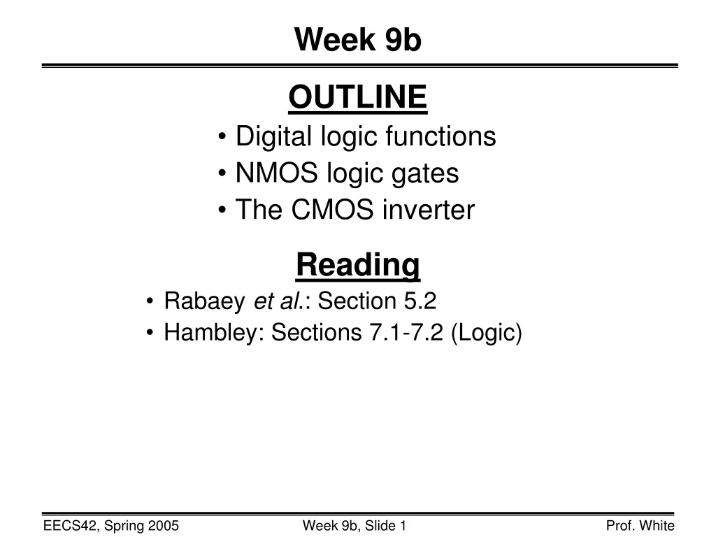
Week 9b OUTLINE • Digital logic functions • NMOS logic gates • The CMOS inverter Reading • Rabaey et al.: Section 5.2 • Hambley: Sections 7.1-7.2 (Logic)
Digital Signals • For a digital signal, the voltage must be within one of two ranges in order to be defined: • Positive Logic: • “low” voltage logic state 0 • “high” voltage logic state 1 VDD VOH “1” VIH increasing voltage undefined region VIL “0” VOL 0 Volts
Logic Functions, Symbols, & Notation TRUTH NAMESYMBOLNOTATIONTABLE A F F = A “NOT” A F F = A+B “OR” B A F F = A•B “AND” B
A F F = A+B “NOR” B A F F = A•B “NAND” B A F F = A + B “XOR” (exclusive OR) B
vIN = VDD VDD/RD increasing vGS = vIN > VT VDD vGS = vin VT NMOS Inverter (“NOT” Gate) Voltage-Transfer Characteristic Circuit: vOUT VDD F A iD vIN 0 VT VDD vDS 0
Definition of Noise Margins logic swing Vsw Noise margin high Noise margin low Noise Margins Definition of Input Levels VOL VOH
NMOS NAND Gate • Output is low only if both inputs are high VDD RD F A Truth Table B
NMOS NOR Gate • Output is low if either input is high VDD RD F A B Truth Table
Disadvantages of NMOS Logic Gates • Large values of RD are required in order to • achieve a low value of VOL • keep power consumption low • Large resistors are needed, but these take up a lot of space. • One solution is to replace the resistor with an NMOSFET that is always on.
VDD S G D VOUT VIN D G S The CMOS Inverter: Intuitive Perspective SWITCH MODELS CIRCUIT VDD VDD Rp VOUT VOUT VOL = 0 V VOH = VDD Rn Low static power consumption, since one MOSFET is always off in steady state VIN = VDD VIN = 0 V
CMOS Inverter Voltage Transfer Characteristic N: sat P: sat VOUT N: off P: lin C VDD N: sat P: lin B D E A N: lin P: sat N: lin P: off 0 VIN VDD 0
N-Channel MOSFET P-Channel MOSFET
increasing VIN VDSp = - VDD VDSp = 0 CMOS Inverter Load-Line Analysis – VGSp=VIN-VDD + VIN = VDD + VGSp – VDSp=VOUT-VDD + VOUT = VDD + VDSp IDn=-IDp VIN = 0 V IDn=-IDp VIN = VDD increasing VIN VOUT=VDSn 0 VDD 0
CMOS Inverter Load-Line Analysis: Region A – VGSp=VIN-VDD + VIN VTn – VDSp=VOUT-VDD + IDn=-IDp IDn=-IDp VOUT=VDSn 0 VDD 0
CMOS Inverter Load-Line Analysis: Region B – VGSp=VIN-VDD + VDD/2> VIN > VTn – VDSp=VOUT-VDD + IDn=-IDp IDn=-IDp VOUT=VDSn 0 VDD 0
CMOS Inverter Load-Line Analysis: Region D – VGSp=VIN-VDD + VDD– |VTp| > VIN > VDD/2 – VDSp=VOUT-VDD + IDn=-IDp IDn=-IDp VOUT=VDSn 0 VDD 0
CMOS Inverter Load-Line Analysis: Region E – VGSp=VIN-VDD + VIN > VDD– |VTp| – VDSp=VOUT-VDD + IDn=-IDp IDn=-IDp VOUT=VDSn 0 VDD 0
i i i The CMOS Inverter: Current Flow during Switching N: sat P: sat V OUT N: off C V P: lin DD V DD S G N: sat P: lin D V V IN OUT B D E A D G N: lin S P: sat N: lin P: off 0 V IN V 0 DD