Nanostructures and Nanomaterials
820 likes | 1.92k Views
Nanostructures and Nanomaterials. NANO51 Foothill College. Overview. Key nanostructures PNPA rubric Why is each structure important? What industries use these structures? For what types of applications?. http://nanotechweb.org/cws/article/tech/17537. Nanostructures. Aerogels

Nanostructures and Nanomaterials
E N D
Presentation Transcript
Nanostructures and Nanomaterials NANO51 Foothill College
Overview • Key nanostructures • PNPA rubric • Why is each structure important? • What industries use these structures? • For what types of applications? http://nanotechweb.org/cws/article/tech/17537
Nanostructures • Aerogels • Biomolecules • Nanocarbon • Composites • Dendrimers • Glasses / ceramics • Hydrogels • Metals and alloys • Nanomagnets • Nanoparticles/ catalysts • Nanostrings • Nanowires • Quantum dots • Self Assembled Monolayers (SAMs) • Silicon structures and MEMS devices • Thin films
PNPA Rubric • For each structure, what is the application? • What are the structures properties? • How was the material fabricated? • How was the material characterized? • How are structure => properties optimized?
PNPA Rubric • Integrated nanomaterials engineering pedagogy • Properties • Applications • Processing • Nanostructure The P-N-P-A Rubric for undergraduate nanomaterials engineering. The inset diagram shows cross-cutting ideas that enable Nano Science Education (NSE)
Aerogels • Aerogel is a manufactured material with the lowest bulk density of any known porous solid. It is derived from a gel in which the liquid component of the gel has been replaced with a gas. • Aerogels are produced by extracting the liquid component of a gel through supercritical drying. This allows the liquid to be slowly drawn off without causing the solid matrix in the gel to collapse from capillary action, as would happen with conventional evaporation. http://en.wikipedia.org/wiki/Aerogel
Space Shuttle tile using alumina-silicate Aerogel The black coating on the tiles is Reaction Cured Glass (RCG) of which tetrasilicide and borosilicate glass are some of several ingredients. RCG is applied to all but one side of the tile to protect the porous silica and to increase the heat sink properties. The coating actually is also absent from a small margin of the sides adjacent to the uncoated (bottom) side. To waterproof the tile dimethylethoxysilane is injected into the tiles by syringe. Densifying the tile with tetraethyl orthosilicate (TEOS) also helps to protect the silica and waterproof. (Reference Wikipedia) http://en.wikipedia.org/wiki/Space_Shuttle_thermal_protection_system
Biomolecular Nanotechnology • Chaperone structures • DNA templating • Synthetic biology • Synthetic proteins • Liposomes and novel cellular structures http://www.chem.uci.edu/~jsnowick/groupweb/index.html
Biomolecules http://www.sciencemag.org/content/333/6041/412/
Nanocarbon Structures • Carbon nanotubes (SWNT) • Multiwalled nanotubes (MWNT) • Graphene • Carbon nanospheres
Functionalized Carbon Nanotubes Structure of Triptycene Orthoquinone (TOQ, A), Schematic Illustration of Attachment of TOQ onto Carbon Nanotubes (B), and Enlarged Tube Ends with Oxygen-Containing Moieties (C) (Reprinted from Nanowerk Website (American Chemical Society)http://www.nanowerk.com/spotlight/spotid=7288.php
Composite Materials • Carbon nanofibers (CNFs), vapor grown carbon fibers (VGCFs), or vapor grown carbon nanofibers (VGCNFs) are cylindrical nanostructures with graphene layers arranged as stacked cones, cups or plates. Carbon nanofibers with graphene layers wrapped into perfect cylinders are called carbon nanotubes. http://en.wikipedia.org/wiki/Carbon_nanofiber
Carbon Nanoonion Nano-onion structure observed in nanospheres, and annealed carbon black (soot). It is thought that the extended nanostructure forms by wrapping of graphene over a fullerene seed-like nanostructure. (Image courtesy CTIC Group)
Dendrimers www.dendritch.com
Dendrimers (Arborols) Synthesis to 2nd generation Arborol - http://en.wikipedia.org/wiki/Dendrimer
Dendrimer Applications "The future of dendritic macromolecules lies in large part with cleverly designed syntheses that can deliver the structures best-suited for interesting applications," Fréchet says. "Our group is deeply involved not only in mission-oriented synthesis but also in learning more about the properties of dendrimers that take full advantage of their precise nanometer size, high functionality, and regular structural features." This light-harvesting dendrimer performs some functions of artificial photosynthesis. White light is gathered through chain-ends that behave like antennae and funneled into a chromophore in the dendrimer's core that then emits a single color of amplified light http://www.lbl.gov/Science-Articles/Research-Review/Magazine/2001/Fall/features/02Dendrimers.html
Glasses and Ceramics • Glasses are similar to polymers in that they are long chains and almost a liquid • Ceramics are metal-nonmetal compounds with typically ionic bonding • Ceramics have high melting points, can be brittle, and typically are non-conductive • Electroceramics can be conductive • Ceramics have high temperature properties
Electroceramics • 950 -1200°C operation • Type 311 (532, 411, 612, M, Scandate by request) • 3-5A/cm2 CW emission • >15A/cm2 Pulsed emission • AL2O3 Insulation, molybdenum body • >>10,000 hours under ideal conditions • Both power leads electrically isolatedfrom outer body • Non gassy • Available from stock • See below for the same units with support legs • Os/Ru (M Type), Os/W, Ir emission enhancing coatings available http://www.cathode.com/c_cathode.htm
Spin Glasses A spin glass is a magnet with frustrated interactions, augmented by stochastic disorder, where usually ferromagnetic and antiferromagnetic bonds are randomly distributed. Its magnetic ordering resembles the positional ordering of a conventional, chemical glass. Spin glasses display many metastable structures leading to a plenitude of time scales which are difficult to explore experimentally or in simulations. It is the time dependence which distinguishes spin glasses from other magnetic systems. Beginning above the spin glass transition temperature, Tc,[1] http://en.wikipedia.org/wiki/Spin_glass
Nanoglass Coatings Hydrophobic coatings on glass help water to bead up, increasing visibility, and helping to promote easier cleaning. Coatings also add mechanical / abrasion resistance, by promoting surfaces that are also scratch resistant. These coatings are typically made from fluoropolymers, or methylated siloxane materials, both deposited as plasma polymerized coatings. Similar products use chemical coatings to create stain resistant surfaces – mostly be preventing water and ionic residue from sticking – and aiding cleaning of the surfaces as well.
Hydrogels • Hydrogel (also called aquagel) is a network of polymer chains that are hydrophilic, sometimes found as a colloidal gel in which water is the dispersion medium. Hydrogels are highly absorbent (they can contain over 99.9% water) natural or synthetic polymers. Hydrogels also possess a degree of flexibility very similar to natural tissue, due to their significant water content. Highly cross-linked polymers, water insoluble but soak up water, can be ‘mechanically interactive’. http://en.wikipedia.org/wiki/Gel
Hydrogels 4:17 p.m., July 18, 2007--University of Delaware scientists have invented a novel biomaterial with surprising antibacterial properties that can be injected as a low-viscosity gel into a wound where it rigidifies nearly on contact--opening the door to the possibility of delivering a targeted payload of cells and antibiotics to repair the damaged tissue. Regenerating healthy tissue in a cancer-ridden liver, healing a biopsy site and providing wounded soldiers in battle with pain-killing, infection-fighting medical treatment are among the myriad uses the scientists foresee for the new technology. Formulating hydrogels as delivery vehicles for cells extends the uses of these biopolymers far beyond soft-contact lenses into an intriguing realm once viewed as the domain of science fiction, including growing bones and organs to replace those that are diseased or injured. http://www.udel.edu/PR/UDaily/2008/jul/gels071807.html
Hydrogel - PNPA • Water insoluble – but soaks of water • Structure and surface chemistry based on cross-linked organic polymers • Hydrogels are highly absorbent they can contain over 99.9% water (natural or synthetic polymers) possess a degree of flexibility very similar to natural tissue • Wound / tissue replacement / engineering • Diapers, contact lenses, breast implants
Metals and Alloys • Grain boundary engineering • High performance alloys • Control chemistry / processing carefully • Increase strength / stiffness, fatigue • Aerospace applications
Metals and Alloys A grain boundary is the interface between two grains, or crystallites, in a polycrystalline material. Grain boundaries are defects in the crystal structure, and tend to decrease the electrical and thermal conductivity of the material. The high interfacial energy and relatively weak bonding in most grain boundaries often makes them preferred sites for the onset of corrosion and for the precipitation of new phases from the solid. They are also important to many of the mechanisms of creep. On the other hand, grain boundaries disrupt the motion of dislocations through a material, so reducing crystallite size is a common way to improve strength, through grain boundary engineering - http://en.wikipedia.org/wiki/Grain_boundary
Nanomagnetic Materials • Nanotechnology used to ‘freeze’ the positions of the atoms in an orientation that aligns the weak magnetic polarization • Nanomagnetic structures are formed by careful control of material composition and processing parameters • Magnetic domain mapping with MFM • Applications in magnetic / data storage
Using a CCS supercomputer, researchers calculated the magnetic structure of a quantum corral nanostructure, which consists of magnetic iron atoms deposited on a copper surface that "corral" copper electrons.- http://www.ornl.gov/info/ornlreview/v37_2_04/article06.shtml
Nanomagnetic Materials MFM – Magnetic Force Microscopy measurements on novel nanomaterials
Nanoparticles and Catalysts • High surface area • Tailored surface chemistry • Added to bulk / composite materials • Metal, ceramic, or polymer • Can also be ‘powder-like’ Dendron conjugated gold nanoparticle - http://www.nist.gov/mml/ceramics/nanomechanical_properties/nanoparticle-metrology.cfm
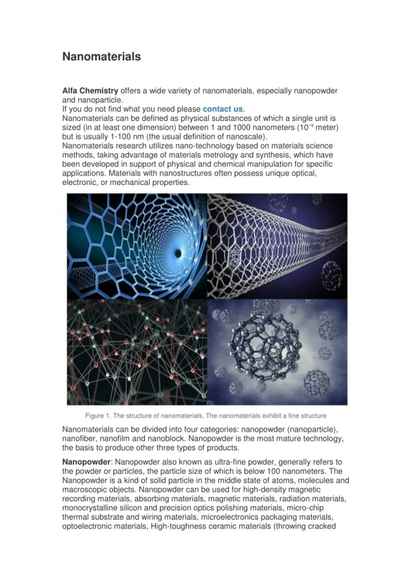
Nanoparticles In nanotechnology, a particle is defined as a small object that behaves as a whole unit in terms of its transport and properties. Particles are further classified according to size[1] : in terms of diameter, coarse particles cover a range between 10,000 and 2,500 nanometers. Fine particles are sized between 2,500 and 100 nanometers. Ultrafine particles, or nanoparticles are sized between 100 and 1 nanometers. Image: TEM (a, b, and c) images of prepared mesoporous silica nanoparticles with mean outer diameter: (a) 20nm, (b) 45nm; and (c) 80nm. SEM (d) image corresponding to (b). The insets are a high magnification of mesoporous silica particle.[1]Reference: http://en.wikipedia.org/wiki/Nanoparticle
Nanowires • A nanowire is a nanostructure, with the diameter of the order of a nanometer (10−9 meters). Alternatively, nanowires can be defined as structures that have a thickness or diameter constrained to tens of nanometers or less and an unconstrained length. At these scales, quantum mechanical effects are important — which coined the term "quantum wires"
Quantum Dots • A quantum dot is a portion of matter (e.g. semiconductor) whose excitons are confined in all three spatial dimensions. Consequently, such materials have electronic properties intermediate between those of bulk semiconductors and those of discrete molecules . Quantum dots are semiconductors whose electronic properties are closely related to the size and shape of the individual crystal. Generally, the smaller the size of the crystal, the larger the band gap, the greater the difference in energy between the highest valence band and the lowest conduction band becomes; more energy is needed to excite the dot, and more energy is released when the crystal returns to its resting state - http://en.wikipedia.org/wiki/Quantum_dot
Quantum Dots Image: TUDelft [Economist]
Quantum Dot Bioconjugates for Ultrasensitive Nonisotopic Detection Warren C. W. Chan and Shuming Nie*Department of Chemistry, Indiana University, Bloomington, IN 47405, USA. ABSTRACT Highly luminescent semiconductor quantum dots (zinc sulfide–capped cadmium selenide) have been covalently coupled to biomolecules for use in ultrasensitive biological detection. In comparison with organic dyes such as rhodamine, this class of luminescent labels is 20 times as bright, 100 times as stable against photobleaching, and one-third as wide in spectral linewidth. These nanometer-sized conjugates are water-soluble and biocompatible. Quantum dots that were labeled with the protein transferrin underwent receptor-mediated endocytosis in cultured HeLa cells, and those dots that were labeled with immunomolecules recognized specific antibodies or antigens. Conceptual diagram of CdSe quantum dot (QD, green spheres with small sphere conjugated attached) interactions with a bacterial cell. Bioconjugated, bare or core-shell, CdSe QDs are subject to abiotic decomposition processes in the vicinity of cells that can lead to heavy metal and metalloid release; released metals and metalloids may be intracellularized, causing toxicity and possibly re-assembling inside cells where they are retained or expelled. http://cfpub.epa.gov/ncer_abstracts/index.cfm/fuseaction/display.abstractDetail/abstract/7390/report/F
Figure 1 (A) Schematic of a ZnS-capped CdSe QD that is covalently coupled to a protein by mercaptoacetic acid. W C W Chan, S Nie Science 1998;281:2016-2018 Published by AAAS
Self Assembled Monolayers • Surface adsorption (Thiol bond to goal) • Post application alignment • Functional end groups • Tailored chemistry • Scaffolding http://en.wikipedia.org/wiki/Self-assembled_monolayer
Self Assembled Monolayers (SAMs) Alkane thiol on gold surface – above schematic diagram – AFM image of oriented thiols http://www3.unict.it/labfsn/images.html
Liposomes Liposomes are composite structures made of phospholipids and may contain small amounts of other molecules. Though liposomes can vary in size from low micrometer range to tens of micrometers, unilamellar liposomes, as pictured here, are typically in the lower size range with various targeting ligands attached to their surface allowing for their surface-attachment and accumulation in pathological areas for treatment of disease.[1]Liposomes are artificially prepared vesicles made of lipid bilayer. Liposomes can be filled with drugs, and used to deliver drugs for cancer and other diseases.[2] Liposomes can be prepared by disrupting biological membranes, for example by sonication. Liposomes can be composed of naturally derived phospholipids with mixed lipid chains (like eggphosphatidylethanolamine) or other surfactants. Liposomes should not be confused with micelles and reverse micelles composed of monolayers.[3]
Silicon Structures / Materials • Wafers • MEMS • LOC • Silicon PV • Biomimetic structures
Silicon Structures / Materials Photovoltaic solar energy represents one of the main components of future sustainable energy scenarios. With high average growth rates of at least 40% p.a. over the last 5 years, and decreasing cost, photovoltaics is expected to become a big business line this century. It is mainly served by (multi-)crystalline silicon. In this context, the Research and Development activities in Germany and the respective states have attained a new intensity and direction. A necessary prerequisite for the further market growth is the development of production processes for increased efficiency and lower cost. Our Institute of Semiconductor Electronics contributes to this field since mid-1998 with several projects on the development of innovative process technologies for the fabrication of photovoltaic devices based on multicrystalline silicon wafers (see design and process optimization). Additionally, we work on new concepts combining multicrystalline silicon wafer technology with thin film emitters, called heterojunction solar cells (see project hetero solar cells) and on totally new concepts for solar cells based on the fusion of nanotechnology and photovoltaics (see photonmanagment and band gap engineering).