Download
1 / 43
430 likes | 451 Views
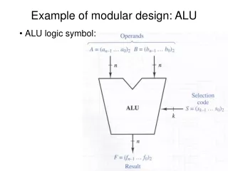
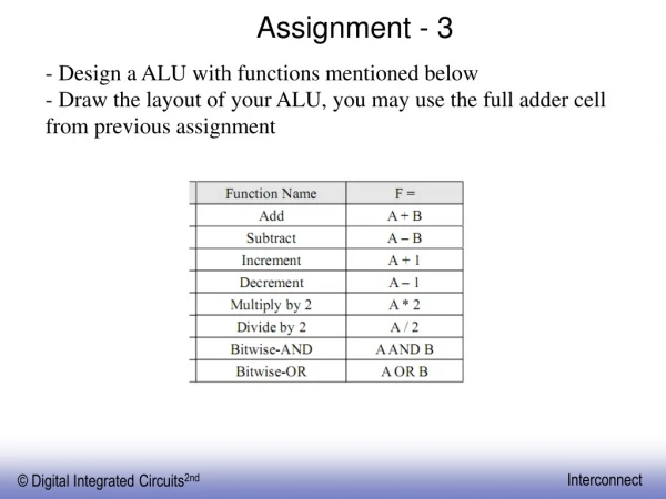
This assignment focuses on designing an Arithmetic Logic Unit (ALU) while considering the impact of interconnect parasitics. The layout will be drawn using a full adder cell from a previous assignment.

E N D
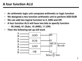
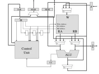
Assignment - 3 • Design a ALU with functions mentioned below • - Draw the layout of your ALU, you may use the full adder cell • from previous assignment
Digital Integrated CircuitsA Design Perspective Jan M. Rabaey Anantha Chandrakasan Borivoje Nikolic Coping withInterconnect December 15, 2002
Impact of Interconnect Parasitics • Reduce Robustness • • Affect Performance • Increase delay • Increase power dissipation Classes of Parasitics • Capacitive • Resistive • Inductive
INTERCONNECT Dealing with Capacitance
Capacitive Cross Talk (Floating lines) capacitor voltage divider network
Capacitive Cross TalkDriven Node 0.5 0.45 0.4 tr↑ X 0.35 C R XY 0.3 Y V Y tXY = RY(CXY+CY) X 0.25 C Y 0.2 V (Volt) 0.15 0.1 0.05 0 0 0.2 0.4 0.6 0.8 1 t (nsec) Keep time-constant smaller than rise time
Dealing with Capacitive Cross Talk • Avoid floating nodes • Protect sensitive nodes from full swing signals • Make rise and fall times as large as possible • Differential signaling (cross talk becomes common mode noise rejected) • Do not run wires together for a long distance • Use shielding wires (GND/VDD) • Use shielding layers (interleave every single layer with a GND or VDD metal plane.
Shielding Shielding wire metal layer 2 GND Shielding V DD layer GND metal layer 1 Substrate ( GND )
Cross Talk and Performance -When neighboring lines switch in opposite direction of victim line, delay increases DELAY DEPENDENT UPON ACTIVITY IN NEIGHBORING WIRES Cc Miller Effect - Both terminals of capacitor are switched in opposite directions (0 Vdd, Vdd 0) - Effective voltage is doubled and additional charge is needed (from Q=CV)
e Interconnect ProjectionsLow-k dielectrics • Both delay and power are reduced by dropping interconnect capacitance • Types of low-k materials include: inorganic (SiO2), organic (Polyimides) and aerogels (ultra low-k) • The numbers below are on the conservative side of the NRTS roadmap
V DD V V in out C L Driving Large Capacitances • Transistor Sizing • Cascaded Buffers
Using Cascaded Buffers In Out CL = 20 pF 1 2 N 0.25 mm process Cin =2.5 fF tp0 = 30 ps F = CL/Cin = 8000 fopt = 3.6 N = 7 tp = 0.76 ns (See Chapter 5)
Trade off Performance for Area and Energy Given tpmax find N and f Area Energy Output Driver Design
How to Design Large/Wide Transistors D(rain) Reduces diffusion capacitance Reduces gate resistance Multiple Contacts S(ource) small transistors in parallel G(ate)
ESD Protection A human walking over a synthetic carpet over in 80% relative humidity can accumulate a voltage potential of 1.5 kV—you have probably experienced the sparks that jump from your hand when touching a metal object under those circumstances. The same is true for the assembly machinery. The gate connection of an MOS transistor has a very high input resistance. The voltage at which the gate oxide punctures and breaks down is about 40-100 V, and is getting smaller with reducing oxide thicknesses. A human or machine, charged up to a high static potential, can hence easily cause a fatal breakdown of the input transistors to happen when brought in contact with the input pin. This phenomena called Electrostatic Discharge (ESD) has proven to be fatal to many circuits during manufacturing and assembly.
ESD Protection • When a chip is connected to a board, there is unknown (potentially large) static voltage difference • Equalizing potentials requires (large) charge flow through the pads • Diodes sink this charge into the substrate – need guard rings to pick it up. Guard rings are grounded p+ diffusions in a p-well and supply-connected n+ diffusions in an n-well that are used to collect injected minority carriers before they reach the base of the parasitic bipolar transistors.
ESD Protection The protection diodes D1 and D2 turn on when the voltage at node X rises above VDD or goes below ground. The resistor R is used to limit the peak current that flows in the diodes in the event of an unusual voltage excursion.
Chip Packaging • Bond wires (~25m) are used to connect the package to the chip • Pads are arranged in a frame around the chip • Pads are relatively large (~100m in 0.25m technology),with large pitch (100m) • Many chips areas are ‘pad limited’
Pad Frame Layout Die Photo
Chip Packaging • An alternative is ‘flip-chip’: • Pads are distributed around the chip • The soldering balls are placed on pads • The chip is ‘flipped’ onto the package • Can have many more pads
Impact of Resistance • We have already learned how to drive RC interconnect • Impact of resistance is commonly seen in power supply distribution: • IR drop • Voltage variations • Power supply is distributed to minimize the IR drop and the change in current due to switching of gates
Electromigration (1) Line-open failure causes the wire to break or to short circuit to another wire
Electromigration (2) Open failure in contact plug
( ) = + + + T 0 . 377 R C 0 . 693 R C R C R C d w w d out d w w out The Global Wire Problem Challenges • No further improvements to be expected after the introduction of Copper (superconducting, optical?) • Design solutions • Use of fat wires • Insert repeaters — but might become prohibitive (power, area) • Efficient chip floorplanning • Towards “communication-based” design • How to deal with latency? • Is synchronicity an absolute necessity?
Diagonal Wiring destination diagonal y source x Manhattan • 20+% Interconnect length reduction • Clock speed Signal integrity Power integrity • 15+% Smaller chips plus 30+% via reduction Courtesy Cadence X-initiative
Reducing RC-delay Making an interconnect line m times shorter reduces its propagation delay quadratically, and is sufficient to offset the extra delay of the repeaters when the wire is sufficiently long. Repeater Assuming that the repeaters have a fixed delay tpbuf, we can derive the delay of the partitioned wire. (chapter 5)
Repeater Insertion (Revisited-ch.5) Sizing the repeaters is needed to reduce the delay. A more precise expression of the delay of the interconnect chain is obtained by modeling the repeater as an RC network, and by using the Elmore delay approach. Assuming that Rd and Cd are the resistance and capacitance of a minimum-sized repeater, and s is the sizing factor, this leads to the following expression:
INTERCONNECT Dealing with Inductance
V DD i ( t ) L V ’ DD V V out in C L GND ’ L L di/dt • Impact of inductance on supply voltages: • Change in current induces a change in voltage • Longer supply lines have larger L
Dealing with Ldi/dt • Separate power pins for I/O pads and chip core. • Careful selection of the positions of the power and ground pins on the package. • Increase the rise and fall times of the off-chip signals to the maximum extent allowable. • Use advanced packaging technologies.
Choosing the Right Pin Careful selection of the positions of the power and ground pins on the package —The inductance of pins located at the corners of the package is substantially higher
Decoupling Capacitors High frequency spike collection • Decoupling capacitors are added: • on the board (right under every supply pin) • on the chip (under the supply straps, near large buffers) low-pass network
l l l l r r r r V V x in out g c g c g c g c The Transmission Line When an interconnection wire becomes sufficiently long or when the circuits become sufficiently fast, the inductance of the wire starts to dominate the delay behavior, and transmission line effects must be considered.
Design Rules of Thumb • Transmission line effects should be considered when the rise or fall time of the input signal (tr, tf) is smaller than the time-of-flight of the transmission line (tflight). tr (tf) << 2.5 tflight • Transmission line effects should only be considered when the total resistance of the wire is limited:R < 5 Z0 • The transmission line is considered lossless when the total resistance is substantially smaller than the characteristic impedance, R < Z0/2
Should we be worried? • Transmission line effects cause overshooting and non-monotonic behavior Clock signals in 400 MHz IBM Microprocessor (measured using e-beam prober) [Restle98]
Matched Termination Z 0 Z Z L 0 Series Source Termination Z S Z Z 0 0 Parallel Destination Termination
Memory Sub-system EmbeddedProcessors Interconnect Backplane Peripherals ConfigurableAccelerators Accelators The “Network-on-a-Chip”