Download

1 / 122
1.53k likes | 2.36k Views
CSE 325 : Computer Peripherals and Interfacing. Sheikh Sujan Ali Associate Professor Dept. of Computer Science and Engineering Jatiya Kabi Kazi Nazrul Islam University Mymensingh , Bangladesh. Introduction. Computer Peripherals

E N D
CSE 325:Computer Peripherals and Interfacing Sheikh Sujan Ali Associate Professor Dept. of Computer Science and Engineering JatiyaKabiKaziNazrul Islam University Mymensingh, Bangladesh
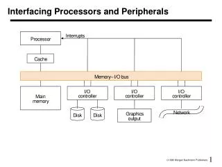
Introduction • Computer Peripherals A computer peripheral is any external device that provides input and output for the computer. For example, a keyboard and mouseare input peripherals, whilea monitor and printerare output peripherals. Computer peripherals, or peripheral devices, are sometimes called I/O devices because they provide input and output for the computer. Some peripherals, such as externalhard drives, USB flash drive and memory cardprovide both input and output for the computer.
Introduction • Computer Interfacing In computing, an interface is an art of connecting computers and peripherals by which two or more separate components of a computer system can exchange information. The exchange can be between software, computer hardware, peripheral devices, humans and combinations of these. The goal of this course is to introduce hardware and software design techniques and issues for interfacing computers and peripheral devices
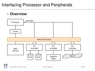
Basic I/O Interface • A microprocessor is great at solving problem, but can not communicate with the outside world. • This chapter outlines some of the basic methods of communications, both serial and parallel, between humans or machines and the microprocessor. • First introduces the basic I/O interface and discuss decoding for I/O devices. • Then, provides detail on parallel and serial interfacing, both of which have a variety of applications.
Basic I/O Interfaces • The basic input device is a set of three-state buffers. • The basic output device is a set of data latches. • The term IN refers to moving data from the I/O device into the microprocessor and • The term OUT refers to moving data out of the microprocessor to the I/O device.
Chapter Objectives Upon completion of this chapter, you will be able to: • Explain the operation of the basic input and output interfaces. • Decode an 8-, 16-, and 32-bit I/O device so that they can be used at any I/O port address. • Define handshaking and explain how to use it with I/O devices. • Interface and program the 82C55 programmable parallel interface. • Interface LCD displays, LED displays, keyboards, ADC, DAC, and various other devices to the 82C55. • Interface an analog-to-digital converter and a digital-to-analog converter to the microprocessor. • Interface both DC and stepper motors to the microprocessor.
The I/O Instructions • One type of instruction*transfers information to an I/O device (OUT). [*In computer science, an instruction is a single operation of a processor defined by the processor instruction set.] • Another reads from an I/O device (IN). • Instructions are also provided to transfer strings of data between memory and I/O. • Instructions that transfer data between an I/O device and the microprocessor’s accumulator (AL, AX, or EAX) are called IN and OUT.
The I/O Instructions • The I/O address is stored in register DX as a 16-bit address or as an 8-bit address. • Intel calls the 8-bit form (p8) a fixed address • The 16-bit address is called a variable address because it is stored in a DX, and then used to address the I/O device. • Other instructions that use DX to address I/O are the INS and OUTS instructions. • I/O ports are 8 bits in width. • a 16-bit port is actually two consecutive 8-bitports being addressed • a 32-bit I/O port is actually four 8-bit ports
The I/O Instructions • When data are transferred using IN or OUT, the I/O address, (port number or simply port), appears on the address bus. • External I/O interface decodes the port number in the same manner as a memory address. • the 8-bit fixed port number (p8) appears on address bus connections A7–A0 with bits A15–A8 equal to 000000002 • The 16-bit variable port number (DX) appears on address connections A15–A0.
The I/O Instructions • INS and OUTS instructions address an I/O device using the DX register. • but do not transfer data between accumulator and I/O device as do the IN/OUT instructions • Instead, they transfer data between memory and the I/O device
Isolated and Memory-Mapped I/O • Two different methods of interfacing I/O: - isolated I/O and - memory-mapped I/O. • In isolated I/O, the IN, INS, OUT, and OUTS transfer data between the microprocessor’s accumulator or memory and the I/O device. • In memory-mapped I/O, any instruction that references memory can accomplish the transfer.
Isolated I/O • The most common I/O transfer techniqueused in the Intel-based system is isolated I/O. • isolated describes how I/O locations are isolated from memory in a separate I/O address space • Addresses for isolated I/O devices, called ports, are separate from memory. • Because the ports are separate, the user can expand the memory to its full size without using any of memory space for I/O devices.
Isolated I/O • A disadvantage of isolated I/O is that data transferred between I/O and microprocessor must be accessed by the IN, INS, OUT, and OUTS instructions. • Separate control signals for the I/O space are developed (using M/IO and W/R ), which indicate an I/O read (IORC) or an I/O write (RD) operation. • These signals indicate an I/O port address, which appears on the address bus, is used to select the I/O device.
Memory and I/O Maps • in the PC, isolated I/Oports are used to control peripheral devices • an 8-bit port address is used to access devices located on the system board, such as the timer and keyboard interface • a 16-bit port is used to access serial and parallel ports, video and disk drive systems Figure: The memory and I/O maps for the 8086/8088 microprocessors. (a) Isolated I/O. (b) Memory-mapped I/O.
Memory-Mapped I/O • Memory-mapped I/O does not use the IN, INS, OUT, or OUTS instructions. • It uses any instruction that transfers data between the microprocessor and memory. • treated as a memory location in memory map • Advantage is any memory transfer instruction can access the I/O device. • Disadvantage is a portion of memory system is used as the I/O map. • reduces memory available to applications
The Basic Input Interface • Three-state buffers are used to construct the 8-bit input port depicted in Figure 2. • External TTL data are connected to the inputs of the buffers. • buffer outputs connect to the data bus • The circuit of allows the processor to read the contents of the eight switches that connect to any 8-bit section of the data bus when the select signal becomes a logic 0.
Figure 2 The basic input interface illustrating the connection of eight switches. Note that the 74ALS244 is a three-state buffer that controls the application of the switch data to the data bus.
The Basic Input Interface • When the IN instruction executes, contents of the switches copy to the AL register. • To interface 16-bit of data, the circuit in Figure 2 is doubled to include to 74ALS244 buffers that connect 16 bits of input data to 16-bit data bus. • To interface 32 bits of data, the circuit is expanded by a factor of 4.
The Basic Output Interface • Receives data from the processor and usually must hold it for some external device. • latches or flip-flops, like buffers in the inputdevice, are often built into the I/O device • Fig 3 shows how eight light-emitting diodes (LEDs) connect to the processor through a set of eight data latches. • The latch stores the number output by the microprocessor from the data bus so that the LEDs can be lit with any 8-bit binary number.
Figure 3 The basic output interface connected to a set of LED displays.
The Basic Output Interface • Latches hold the data because when the processor executes an OUT, data are only present on the data bus for less than 1.0 µs. • the viewer would never see the LEDs illuminate • When the OUT executes, data from AL, AX, or EAX transfer to the latch via the data bus. • Each time the OUT executes, the SEL signal activates, capturing data to the latch. • data are held until the next OUT • When the output instruction is executed, data from the AL register appear on the LEDs.
Handshaking • Many I/O devices accept or release information slower than the microprocessor. • A method of I/O control called handshaking or polling, synchronizes the I/O device with the microprocessor. • An example is a parallel printer that prints a few hundred characters per second (CPS). • The processor can send data much faster. • a way to slow the microprocessor down to match speeds with the printer must be developed
Handshaking • Fig 4 illustrates typical input and output connections found on a printer. • data transfers via data connections (D7–D0) • ASCII data are placed on D7–D0, and a pulse is then applied to the STB connection. • BUSY indicates the printer is busy • STB is a clock pulse used to send data to printer • The strobe signal sends or clocks the data into the printer so that they can be printed. • as the printer receives data, it places logic 1 on the BUSY pin, indicating it is printing data
Figure 4 The DB25 connector found on computers and the Centronics 36-pin connector found on printers for the Centronics parallel printer interface.
Handshaking • The software polls or tests the BUSY pin to decide whether the printer is busy. • If the printer is busy, the processor waits • if not, the next ASCII character goes to the printer • This process of interrogating the printer, or any asynchronous device like a printer, is called handshaking or polling.
Input Devices • Input devices are already TTL and compatible, and can be connected to the microprocessor and its interfacing components. • or they are switch-based • Switch-based devices are either open or connected; These are not TTL levels. • TTL levels are a logic 0 (0.0 V–0.8 V) • or a logic 1 (2.0 V–5.0 V) • Using switch-based device as TTL-compatible input requires conditioning applied.
Input Devices • Fig 5shows a toggle switch properly connected to function as an input device. • A pull-up resistor ensures when the switch is open, the output signal is a logic 1. • when the switch is closed, it connects toground, producing a valid logic 0 level • A standard range of values for pull-up resistors is between 1K Ohm and 10K Ohm.
Input Devices Figure 5 A single-pole, single-throw switch interfaced as a TTL device.
Input Devices • Mechanical switch contacts physically bounce when they are closed, • which can create a problem if a switch is usedas a clocking signal for a digital circuit • To prevent problems with bounces, one of the circuits shown in Fig 7can be used. • the first is a classic textbook bounce eliminator • second is a more practical version of the same • The first version costs more to construct • the second costs requires no pull-up resistorsand two inverters instead of two NAND gates
Bouncing Problem Switch Bouncing in Pull Down Connection Switch Bouncing in Pull Up Connection
Figure 6Debouncing switch contacts: (a) conventional debouncing and (b) practical debouncing. • as the Q input from the switch becomes a logic 0, it changes the state of the flip-flop • if the contact bounces away from the Q input, the flip-flop remembers, no change occurs, and thus no bounce
Output Devices • Output devices are more diverse than input devices, but many are interfaced in a uniform manner. • Before an output device can be interfaced, we must understand voltages and currents from the microprocessor or TTL interface. • Voltages are TTL-compatible from the microprocessor of the interfacing element. • logic 0 = 0.0 V to 0.4 V • logic 1 = 2.4 V to 5.0 V
Output Devices • Currents for a processor and many interfacing components are less than for standard TTL. • Logic 0 = 0.0 to 2.0 mA • logic 1 = 0.0 to 400 µA • Fig 8 shows how to interface a simple LED to a microprocessor peripheral pin. • a transistor driver is used in 8
Output Devices Figure 8 Interfacing an LED: using a transistor and.
Output Devices • TTL input signal has minimum value of 2.4 V • Drop across emitter-base junction is 0.7 V. • The difference is 1.7 V • the voltage drop across the resistor • The value of the resistor is 1.7 V ÷ 0.1 mA or 17K W. • as 17K W is not a standard value, an 18K W resistor is chosen
Output Devices • In 8, we elected to use a switching transistor in place of the TTL buffer. • 2N2222 is a good low-cost, general-purpose switching transistor with a minimum gain of 100 • collector current is 10 mA; so base current willbe 1/100 of collector current of 0.1 mA • To determine the value of the base current–limiting resistor, use the 0.1 mA base current and a voltage drop of 1.7 V across the base current–limiting resistor.
Output Devices • Fig 9 illustrates a motor connected to the Darlington-pair with a minimum current gain of 7000 and a maximum current of 4A. • Value of the bias resistor is calculated exactly the same as the one used in the LED driver. • The current through the resistor is 1.0 A ÷ 7000, or about 0.143 mA. • Voltage drop is 0.9 V because of the two diode drops (base/emitter junctions). • The value of the bias resistor is 0.9 V ÷ 0.143 mA or 6.29K W.
Figure 9 A DC motor interfaced to a system by using a Darlington-pair. • The Darlington-pair must usea heat sink because of theamount of current • the diode must be present toprevent the Darlington-pairfrom being destroyed by inductive kickback
Darlington pair • Darlington pair/transistor is a compound structure of a particular design made by two bipolar transistors connected in such a way that the current amplified by the first transistor is amplified further by the second one. • Darlington transistors can be used in high-current circuits, such as those involving computer control of motors or relays.
Decoder In digital electronics, a binary decoder is a combinational logic circuit that converts binary information from the n coded inputs to a maximum of 2n unique outputs.
Decoding 8-Bit I/O Port Addresses • Fixed I/O instruction uses an 8-bit I/O port address that on A15–A0 as 0000H–00FFH. • we often decode only address connectionsA7–A0 for an 8-bit I/O port address • The DX register can also address I/O ports 00H–FFH. • If the address is decoded as an 8-bit address, we can never include I/O devices using a 16-bit address. • the PC never uses or decodes an 8-bit address
Decoding 8-Bit I/O Port Addresses • Figure 10 shows a 74ALS138 decoder that decodes 8-bit I/O ports F0H - F7H. • identical to a memory address decoder exceptwe only connect address bits A7–A0 to theinputs of the decoder • Figure 11 shows the PLD version, using a GAL22V10 (a low-cost device) for this decoder. • The PLD is a better decoder circuit because the number of integrated circuits has been reduced to one device.
Figure 10 A port decoder that decodes 8-bit I/O ports. This decoder generates active low outputs for ports F0H–F7H.
Figure 12 A PLD that decodes 16-bit I/O ports EFF8H through EFFFH.
Figure 13 A 32-bit-wide port decoded at 70H through 73H for the 80486DX microprocessor. • I/O ports decoded by this interface are the 8-bit ports 70H–73H • When writing to access this port, it is crucial to use the address 70H for 32-bit input • as instruction IN EAX, 70H
THE PROGRAMMABLE PERIPHERAL • 82C55 programmable peripheral interface (PPI) is a popular, low-cost interface component found in many applications. • The PPI has 24 pins for I/O, programmable in groups of 12 pins and groups that operate in three distinct modes of operation. • 82C55 can interface any TTL-compatibleI/O device to the microprocessor.
THE PROGRAMMABLE PERIPHERAL • The 82C55 (CMOS version) requires wait states if operated with a processor using higher than an 8 MHz clock. • also provides at least 2.5 mA of sink (logic 0) current at each output, a maximum of 4.0 mA • Because I/O devices are inherently slow, wait • states used during I/O transfers do not impact significantly upon the speed of the system. • The 82C55 still finds application even in the latest Core2-based computer system.
THE PROGRAMMABLE PERIPHERAL • 82C55 is used for interface to the keyboard and parallel printer port in many PCs. • found as a function within an interfacing chip set • also controls the timer and reads data from the keyboard interface • An experimentation board is available that plugs into the parallel port of a PC, to allow access to an 8255 located on the board. • The 8255 is programmed in either assembly language or Visual C++ through drivers available with the board.
Basic Description of the 82C55 • Fig 14 shows pin-outs of the 82C55 in DIP and surface mount (flat pack) format. • The three I/O ports (labeled A, B, and C) are programmed as groups. • group A connections consist of port A (PA7–PA0) and the upper half of port C (PC7–PC4) • group B consists of port B (PB7–PB0) and the lower half of port C (PC3–PC0) • 82C55 is selected by its CS pin for programming and reading/writing to a port.