Download
1 / 11
110 likes | 135 Views
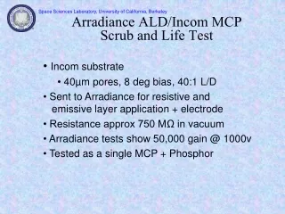
Detailed analysis of ALD MCP substrate with 40μm pores, 8° bias, 40:1 L/D ratio sent to Arradiance for electrode application. Resistance at 750 MΩ, 50,000 gain shown at 1000v. Scrub and life tests conducted. Pre/post-scrub images, histograms, and cross-sections demonstrate improvement in MCP performance.

E N D
Arradiance ALD/Incom MCPScrub and Life Test • Incom substrate • 40µm pores, 8 deg bias, 40:1 L/D • Sent to Arradiance for resistive and emissive layer application + electrode • Resistance approx 750 MΩ in vacuum • Arradiance tests show 50,000 gain @ 1000v • Tested as a single MCP + Phosphor
ArradianceALD/Incom MCP Test UV light 550v Bright scratch on phosphor 1000v background, no obvious hotspots other than phosphor defects
ArradianceALD/Incom MCP Lifetest SSL-UCB Arradiance, Inc. 10 mm pore NO LEAD glass substrate, 40:1 L/D, Bias = 880V, Iout~0.4 pA/pore, gain under electron bombardment Tremsin - LAPD workshop 25mm 40µm 40:1 ALD MCP, UV scrub Starts at Bias = 700V, gain x1000, 0.6µA, change to 880v, 0.8µA at 0.03C/cm2 Note: no vacuum bake
“Low” Gain Images Note that the camera used for post scrub imaging was much higheroptical resolution, so differences are exaggerated Pre-Scrub VMCP = 550V Post-Scrub VMCP = 700V
Pre & Post Scrub Histograms at “low” gain Note that the camera used for post scrub imaging was much higheroptical resolution, so differences are exaggerated Pre-Scrub Cross-Section: VMCP = 550V Post-Scrub Cross-Section: VMCP = 700V
“High” Gain Images Note that the defects are present before and after thescrub, most likely dust, and may have charged up topresent the bright rings only when light is turned on! Pre-Scrub VMCP = 900V Post-Scrub VMCP = 1100V
Pre & Post Scrub Histograms at “high” gain Pre-Scrub Cross-Section: VMCP = 900V Post-Scrub Cross-Section: VMCP = 1100V
Pre-Scrub Close-Up • 40µm pores visible • We can see the Hex boundary distortions are uneven • 800v MCP • 2900v screen Post scrub at 800v
Post-Scrub Close-Up • 40µm pores still visible but are now narrow spots. • Hex boundary distortions are washed out • 1100v MCP • 2900v screen • Former dead spots now have bright halos at high gain
Background Images No significant changes Pre-Scrub VMCP = 1000V Post-Scrub VMCP = 1100V
Post-Scrub response at higher gain Modulation seems more related to applied voltage - not gain. VMCP = 600V VMCP = 700V VMCP = 800V VMCP = 900V VMCP = 1000V VMCP = 1100V