Download
1 / 11
110 likes | 208 Views
Explore the advancements in Digital CFEB technology for improving particle flux handling, trigger readout capabilities, and latency constraints. Evaluate ADC options, interface challenges, and drive considerations for enhanced performance.

E N D
Digital CFEB (an Update) Ben Bylsma The Ohio State University B. Bylsma, EMU at CMS Week, March 16, 2009
SLHC Phase 1 Upgrade Fully Instrument ME4/2 Chambers August 2009 Install/Instrument ME4/2 Test Chambers B. Bylsma, EMU at CMS Week, March 16, 2009
OSU Digital CFEB • Replace SCA with Flash ADCs/Memories • Better rate capability • Similar Cost • Propose 514 new cards ME1/1a • Old cards to populate ME4/2 Upgrade • Handle highest particle flux • Restore ME1/1a triggering and • readou t to range 2.1-2.4 B. Bylsma, EMU at CMS Week, March 16, 2009
Current CFEB Basic Block Diagram: SCA ADC FPGA To DMB over Skewclear + 8 Triad signals pre 12 bits 16 16 Chan-link - ref mux 21 bits 6 layers 21:3 280 Mbps . . . . . . To TMB over Skewclear comp pre 3x8 2:1 LVDS 24 bits 80 MHz . . . . . . 3x8 6 layers Time Line: Digitization and Readout Analog storage Analog storage - no coincidence Analog storage with L1A*LCT coincidence event LCT L1A ~3.2µS Release Caps ~20µS Analog samples are stored until L1A. Then ADC must digitize 8X16 samples one at a time. Limited number of capacitors and single channel ADC impose constraints on LCT and L1A latencies. B. Bylsma, EMU at CMS Week, March 16, 2009
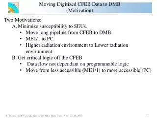
New Digital CFEB Basic Block Diagram: Serial LVDS 8 pairs ref ADC ADC FPGA + + 8 Triad signals 8 16 8 16 pre To DMB over Fiber 16 pairs - - Pipeline/FIFOs Serial MGT Opt. Trnscvr 8 pairs ~1Gbps ref To TMB over Skewclear . . . 6 layers Serial MGT Opt. Trnscvr . . . ~2Gbps comp pre 48 . . . . . . 6 layers Digitization Latency Readout Time Line: Pipeline FIFO FIFO event xfer LCT L1A ~3.2µS ~20µS No Dead Time. All 96 channels continuously digitized (no multiplexing). B. Bylsma, EMU at CMS Week, March 16, 2009
First Step – Choose ADC • ADC choice drives subsequent design considerations • Interface between pre-amp and ADC • Voltage/Power requirements • Could impact LVDB design • ADC choices:(8 ch, 12 bit, 20-65 MSPS, Serial LVDS output) • MAX1437 (Maxim) 1.8V supply, 1.4Vpp range • ADC12EU050 (National) 1.2V supply, 2.1Vpp range • AD9222 (Analog Devices) 1.8V supply, 2Vpp range • ADS5281 (Texas Instr.) 3.3V analog, 1.8V digital, 2Vpp range B. Bylsma, EMU at CMS Week, March 16, 2009
Issues with ADCs • None are suitable drop-in replacements for SCA/ADC • ADC’s • All have differential inputs • Limits on common mode • Have internal input bias network • Pre-Amp • Single ended output • Limited range of baseline level • Designed to drive small capacitive load • Pre-Amp/ADC Interface • Mnfr. suggest transformer coupling • (not an option for us) • Amplifier to generate differential signal • (requires 96 amplifiers) • Direct couple single ended signal • (common mode consequences) • (level shifting/scaling) • AC couple single ended signal • (common mode consequences) • (no level shifting, but still have biasing to consider) B. Bylsma, EMU at CMS Week, March 16, 2009
Evaluation Boards • Purchased Evaluation Boards for ADS5281 and AD9222 • Basic Setup: Logic Analyzer Input Circuitry ADC DeSer + - • Identify constraints/operation limits of ADC • Direct Coupling Concerns • Common Mode • Data Sheet: Vcm = 1.5±0.05V • How far from nominal? • Baseline Level • Range • Digital output range is 2V • But is linear range of common mode 2V? • AC Coupling Concerns • Same as direct coupling • No worries with pre-amp baseline level • But need to bias positive input B. Bylsma, EMU at CMS Week, March 16, 2009
Constraints (ADS5281) • ADC Constraints: • Vcm -600mV < (IN+ + IN-)/2 < Vcm +300mV (1.8Vpp on IN+) • (IN- -1V) < IN+ < (IN-+1V)(ADC output range) • Pre-Amp Constraints: • Baseline Level • Currently 1.8V • Max ~2.0V • Min ~1.2V (maybe 1.0V) • Drive Capability • Small (few mA at best) • Scaling: • Scale down input • Add digital gain on output • Resistor divider 1.2k Vcm 1.2k B. Bylsma, EMU at CMS Week, March 16, 2009
Digitize Amplifier Pulses Connect CFEB to Evaluation Board: 50ns samples B. Bylsma, EMU at CMS Week, March 16, 2009
Current DCFEB R&D Status • Evaluating ADC • Exploring Options for Interfacing to ADC • Direct Coupling • AC Coupling • Amplifier Coupling • Scaling B. Bylsma, EMU at CMS Week, March 16, 2009