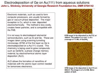
Download
1 / 1
10 likes | 140 Views
(111). (113). (114). Growth Behavior of Ge Quantum Dots on the Nano-sized Si(111) surface bounded by the (100) facets. S.-S. Ferng and D.-S. Lin Institute of Physics, National Chiao-Tung University, Hsinchu 300, Taiwan.

E N D
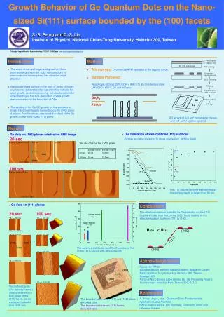
(111) (113) (114) Growth Behavior of Ge Quantum Dots on the Nano-sized Si(111) surface bounded by the (100) facets S.-S. Ferng and D.-S. Lin Institute of Physics, National Chiao-Tung University, Hsinchu 300, Taiwan This paper is published at Nanotechnology 17, 5207 ( 2006) as a front cover page featured article. Introduction Method • The strain-driven self-organized growth of three-dimensional quantum-dot (QD) nanostructure in semiconductor heteroepitaxy has attracted much attention . • Nanoscale-sized surface in the form of mesa or ridges on patterned substrates offer opportunities not only for novel growth-control engineering, but also fundamental understanding of the size-dependent crystal growth phenomena during the formation of QDs. . • The studies of the Ge QD growth on the windows or mesas have been largely conducted on the (100) plane of silicon. Few literatures discussed the effect of the Ge growth on the nano-sized (111) plane. • Microscopy: Commercial AFM operated in the tapping mode. • Sample Prepared: Anisotropic etching: 20% KOH + IPA (5:1) at room temperature UHVCVD: 650℃, 20 and 100 sec Ge2H4 5 sccm 2D arrays of 3×6 μm2 rectangular mesas and 1×1 μm2 negative pyramid. Results • The formation of well-confined (111) surfaces • Ge dots on (100) planes: derivative AFM image 20 sec Profiles and slop angles of Si mesa sidewall vs. etching depth Etching depth= 120 nm 300 nm 500 nm The Ge dots on the (100) plane (111) (100) (100) 5 μm× 5 μm 100 sec Ge dot Etching depth= 80 nm 970 nm 420 nm 150 nm the (111) facets become well-defined as the etching depth is larger than 80 nm. 5.5 μm× 5.5 μm • Ge dots on (111) planes Conclusions The effective chemical potential for Ge adatoms on the (111) facet is smaller than that on the (100) facet, leading to the effective adatom flux from (111) to (100). 20 sec 100 sec W111= 150 nm W111= 100 nm μ100 μ111 < (100) 400 nm× 400 nm W111= 180 nm W111= 370 nm (111) (100) (100) (111) The volumes distribution and the thickness of Ge on the (111) planes with different width. (100) W111= 530 nm Acknowledgements W111= 610 nm Tsung-Hsi YANG Microelectronics and Information Systems Research Center, National Chiao Tung University, Hsinchu 300, Taiwan Guangli LUO National Nano Device Laboratories, No. 26, Prosperity Road 1, Science-base Industrial Park, Taiwan 300, R.O.C. (100) (111) (100) W111= 1190 nm Nuclei-free bands (the denuded zone ) clearly observed on both edge of the (111) facets, as an example marked in blue dash line. References A. Bruce, Joyce, et al.: Quantum Dots: Fundamentals, Applications, and Frontiers, NATO science series. 190 (Springer, Dordrecht, 2005) and reference therein. The boundaries between (111) and (100) planes : denuded zone The boundaries between (111) facets: denuded zone