Advanced Techniques in Programmable Circuit Calibration and Adaptation for Enhanced Performance
This document explores advanced applications in electronic design, focusing on programmable compensation techniques for analog circuits, high-speed digital circuits, and automated discovery via evolutionary algorithms. Key topics include clock skew compensation, robust fault tolerance, and adaptation to extreme temperature environments. Emphasis is placed on the evolution of controllers and adaptive filters, alongside innovative uses of EDA tools in analog circuit design. The results illustrate significant improvements in calibration accuracy, yield rates, and overall circuit efficiency, advancing the field of electronic hardware.

Advanced Techniques in Programmable Circuit Calibration and Adaptation for Enhanced Performance
E N D
Presentation Transcript
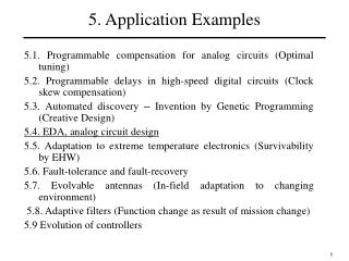
5. Application Examples 5.1. Programmable compensation for analog circuits (Automated Calibration, Optimal tuning, Parameter adjustment) 5.2. Programmable delays in high-speed digital circuits (Clock skew compensation) 5.3. Automated discovery/invention by Evolutionary Algorithms (Creative Design) 5.4. EDA Tools, analog circuit design 5.5. Adaptation to extreme temperature electronics (Survivability by EHW) 5.6. Fault-tolerance and fault-recovery 5.7. Evolvable antennas (In-field adaptation to changing environment) 5.8. Adaptive filters (Function change as result of mission change) 5.9 Evolution of controllers 1
Analogue EHW chip for cellular phones –Higuchi, Japan • Off-line analogue EHW • Intermediate Frequency Filter • Analogue Band-pass Filter • Must be compact and fast: LSI required • Large market • Variations in analogue components performance are adjusted by GA. • Installed in cellular phones since Dec. 2001. From presentation by T. Higuchi, Japan, at EH-2003
Process Variations in Analog LSIs • Values of the manufactured analog circuit components differ from the precise specifications • Poor yield rates especially for high-end analogue circuits e.g. IF filter: a 1% discrepancy from the center frequency unacceptable From presentation by T. Higuchi, Japan, at EH-2003 3
Cures • AI/GA Approach • Use GA to control calibration • Provide many adjustment/calibration points in the circuit • Improved Yield Rates • adjustment for each circuit • Smaller Circuits • use of smaller size analog components • Less Power Consumption Conventional Approach • Use “large” analog components • Manufacturing error due to process variations becomes relatively small • Price: • Higher manufacturing cost • Greater power consumption • Calibration at a LSI tester • a few seconds per a chip From presentation by T. Higuchi, Japan, at EH-2003 Mass-Production 4
Gm amplifier Bias Current Transconductance value: Variations by up to as much as 20% Calibration by varying bias currents From presentation by T. Higuchi, Japan, at EH-2003 5
Review: Transconductance amplifiers • The OTA is a transconductance type device, which means that the input voltage controls an output current by means of the device transconductance, labeled gm. What is important and useful about the OTA’s transconductance parameter is that it is controlled by an external current, the amplifier bias current, IABC. • Active filters are a standard application of the op-amp which can benefit greatly from the controllability of the OTA. What makes the OTA so attractive in these circuits is the ability to form filter circuits with voltage-variable control (via the IABC input) over a n umber of key performance parameters of the filter. The controlled parameter can be the midband gain of the circuit. Alternatively, OTA-based active filters can use the external bias setting to control the location of the critical frequency, or 3-dB frequency, in a filter. The next logical step in controllability is the provision for independent gain and critical frequency setting. A number of other active filters can be realized with th e OTA. These provide the ability to not only change the critical frequency, the gain, or both, but also to preserve the shape of the response. For instance, one might want to control the critical frequency of the filter, but without altering the passband ripple. It is even possible to change the type of response from lowpass to allpass to highpass by continuous adjustment of the transconductance gm. • http://et.nmsu.edu/~etti/winter98/electronics/grise/wrg.html 6
Calibration by GA 0 1 0 0 1 1 0 1 0 0 1 The bias currents can be varied subtly. Bias Current i 100 i 4 i i Register 2 0 0 0 0 Configuration Bits Bias Current Controller The GA seeks the optimal configuration bits. evaluation : the measured gain and group delay From presentation by T. Higuchi, Japan, at EH-2003 7
GA-calibrated IF filter IF filter LSI evaluation IF filter G m GA Software on LSI Tester 4 IN G G G m m m Search Points 1 2 3 i i i i B3 B1 B4 B2 Calibration 0 1 0 0 1 1 0 1 0 0 1 Register 0 1 0 0 1 1 0 1 0 0 1 Configuration Bits Download OUT ( Gm : Transconductance Amplifier ) From presentation by T. Higuchi, Japan, at EH-2003 8
Gm-C IF Filter LSI • Intermediate Frequency Filter • Center Frequency : 455kHz • Bandwidth : 21kHz • 39 Gm amplifiers within the filter • GA calibrate all Gm values to conform to the specifications From presentation by T. Higuchi, Japan, at EH-2003 9
Specifications for the IF filter 0 -4 -8 -12 -16 -20 0 -10 -20 -30 -40 -50 -60 -70 Spec. ( -3dB Points) Gain (dB) Gain (dB) Ideal Response Ideal Response 440 445 450 455 460 465 470 420 430 440 450 460 470 480 490 Frequency (kHz) Frequency (kHz) Group delay : less than 20 usec From presentation by T. Higuchi, Japan, at EH-2003 10
Filter Architecture Configuration Bits Bias Current Controller PLL CLK Filter 1 w0,…,w5 Q0,…,Q5 a0 Filter 3 w12,…,w17 Q12,…,Q17 a2 Filter 2 w6,…,w11 Q6,…,Q11 a1 IF IN IF OUT 39 parameters Gm values w0,…,w17 center freq. Q0,…,Q17 band width a0,…,a2 filter gain 6th order Gm-C filter From presentation by T. Higuchi, Japan, at EH-2003 11
Calibration Experiments After Calibration Spec. Gain Before Calibration 29 out of the 30 test chips could be calibrated (No chip could meet the spec. without calibration!) Frequency Yield : 97% From presentation by T. Higuchi, Japan, at EH-2003 12
Results of GA-calibrated IF Filter Chip Filter 1 PLL Filter 2 Filter 3 DAC Filter area was reduced by 63% Power dissipation reduced by 26% Yield rates improved (97%) This approach can be applied to a wide variety of analog circuits Good approach for low feature size! Photo of the die From presentation by T. Higuchi, Japan, at EH-2003 13