Download
1 / 18
250 likes | 581 Views
Microscale Heat Transfer in Semiconductor Devices Rajeev Ram Peter Mayer, Dietrich Lueerssen, Maryam Farzaneh, Janice Hudgings. Thermal signature of signal inside devices Phonon limits to information capacity of codes. SOA 1. SOA 4. P in. (wave. optical. (wave. waveguide. SOA 6.

E N D
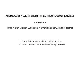
Microscale Heat Transfer in Semiconductor Devices Rajeev Ram Peter Mayer, Dietrich Lueerssen, Maryam Farzaneh, Janice Hudgings • Thermal signature of signal inside devices • Phonon limits to information capacity of codes
SOA 1 SOA 4 Pin (wave optical (wave waveguide SOA 6 SOA 2 guide) amplifier detector guide) SOA 5 Pout SOA 3 position ΔTs position Thermal Profiling of Integrated Circuits Semiconductor Optical Amplifier Pin Pout Optical Regenerator
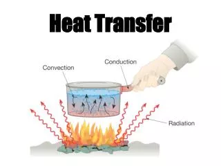
Ts-Ths Pcond = ZT Ts – Ths IV = + Aeff¢ h (Ts –Ta) + Prad ZT Thermal Transport Mechanisms Conduction Convection Dissipated Electrical Power Rseries Ta Ts Pel Ts IV´ Ths Pconv = Aeff.h (Ts – Ta) Pel = IV = IV´ - I2 Rseries Radiated Power Pout Pin Pel = Pcond + Pconv + Prad Prad= Pout - Pin • We can directly measure: • Ta, Ts, Ths (e.g. by micro-thermocouples) • I, V K.P. Pipe and R. J. Ram, IEEE PTL, 2003.
Thermal Profiling of SOAs D. Luerssen, et. al., IEEE PTL, July. 2004. D. Luerssen, et. al., LEOS 2005
Thermal Imaging Trigger at 4f CCD Detector Phase Locked Illumination Source (LED) Microscope Objective Device Temperature modulation at f
-4 x 10 Quantized (measured) signal 8 6 4 DR/R 2 Reflected (actual) signal 0 0 0.2 0.4 0.6 0.8 1 Time (a.u.) -4 Noise Enhanced Dynamic Range low noise x 10 noise injection 8 Quantization steps 6 DR/R 4 2 0 0 0.2 0.4 0.6 0.8 1 Time (a.u.)
Measurement of Thermoreflectance Coefficient Polysilicon b= - 10.11 x 10⁻⁴ 1/K 0 20 40 Doped silicon b= + 2.20 x 10⁻⁴ 1/K mm 60 80 100 Undoped silicon b= + 1.36 x 10⁻⁴ 1/K 120 0 50 100 150 200 mm 150 Phase Image • Green LED used (centered on 525 nm) • for this measurement, each of the thermoreflectance coefficients for can be obtained simultaneously • signs can be obtained from knowledge of sign of one of the materials (here intrinsic Si) 0 100 50 50 mm 0 -50 100 -100 0 50 100 150 200 mm -150
-4 x 10 2 -4 x 10 2 1.5 1.5 1 Thermoreflectance DR/R 1 0.5 0 50 100 150 200 250 300 DR/R 0.5 mm 0 0 0.02 0.04 0.06 0.08 RMS power (W) Thermoreflectance Imaging Validation (Si Resistor) Power MOSFET
180° Phase Shift Thermoreflectance: Single SOA R/R Joule Heating Optical Cooling 8 K 0 300 mK P = 0 P = 1.3 mW in in I = 120 mA I =180 mA I =300 mA 0 0 l =1550 nm in
SOA 1 SOA 4 SOA 6 SOA 2 SOA 5 SOA 3 Thermoreflectance: PIC Joule Heating i = 83 A/m i = 55 A/m i = 55 A/m i = 25 A/m i = 28 A/m Can quantify Joule heating and observe heat spreading.
SOA 2 SOA 4 SOA 1 SOA 3 Power Distribution in SOA-MZI SOA2 SOA4 SOA1 SOA3 Fiber-coupling loss ≈ 5 dB
Cross-plane thermoreflectance imaging: Peltier effect in bulk (Bi2Te3) Direction of applied current (sinusoidal) and heat flow Photomicrograph mm Polycrystalline Bi2Te3 Cu contacts mm Phase(DR/R) Image Log10 |DR/R| Image mm mm mm mm
Polycrystalline structure of Marlow Bi2Te3 Peltier phase crossing (20x objective) • Marlow Bi2Te3 composed of ~10 mm packed crystals • polycrystalline sample difficult to planarize, giving rise to “noisier” images • Doping and orientation of grains can change local b • But b can be defined in an average sense (zoom)
2 2 1 1 0 0 0 100 200 300 400 500 0 100 200 300 400 500 Cross-plane Thermoreflectance Averaged profiles (0.5 Hz 2 A current) Peltier (signal at excitation frequency) Joule (signal at 2 x excitation frequency) |DT| (DC theory) |DT| (DC theory) 0 0 100 100 mm mm 200 200 300 300 0 100 200 300 400 500 0 100 200 300 400 500 2 |DT| (K) |DT| (K) 0.5 1 0 0 0 100 200 300 400 500 0 100 200 300 400 500 50 50 0 0 Phase(DR/R) Phase(DR/R) -50 -50 0 100 200 300 400 500 0 100 200 300 400 500 mm mm
0 2 4 4.9 mm 6 8 metal substrate 10 mm epi 12 14 0 5 10 15 20 mm Best in Class Results 300 • ErAs (SL+substrate) • SiGe (SL+substrate) • BiTe (bulk) • PbTe (n QDSL) SiGe PbTe 250 ErAs 200 150 VOC/DT (mV/K) BiTe 100 50 0 0 50 100 150 200 250 300 350 DT (K) 160x(10nm (InGaAs)0.6(InAlAs)0.4/20nm (n-InGaAs)0.97Er0.03) on 474 mm doped InP substrate
metal epi 4.9 mm -3 x 10 substrate 3 2 -3 x 10 1 1.2 0 0.8 0.4 0 10 20 30 40 0 Cross-plane Thermoreflectance Averaged profiles (5.5 Hz 5 A current) Joule heating (2w) Peltier heating/cooling (w) Magnitude Magnitude 180 Phase 180 Phase 0 0 -180 -180 0 10 20 30 40 mm mm
- V QD Monolayer - - Ag +V Mg:Ag 40 nm Alq (ETL) 3 60 nm TPD (HTL) ITO Glass Nanoparticle Based Illumination and Display Coe-Sullivan (Bulovic Group) Emission Linewidth Color Saturation Difficult to achieve with existing yellow LED technology because only 2.5nm chromaticity drift is allowable throughout temperature range of -20 to +40°C. dE/dT Color Stability
Voltage/PL Intensity 0/min 1/max Time/Wavelength Optical Barcodes Smart Bead Luminex www.qdots.com Illumina Using 4 Intensity levels and 4 colors Correct decode = 90% Incorrect decode = 2% 44 = 256 codes