Download
1 / 22
581 likes | 2.65k Views
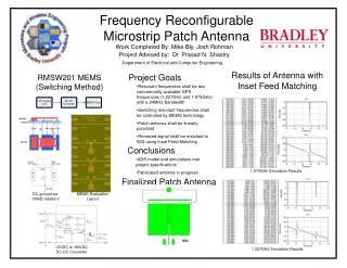
Reconfigurable Patch Antenna. With Matching Network. Presented by: Mike Bly, Josh Rohman Advisor: Dr. Prasad N. Shastry. Presentation Outline. Introduction to Reconfigurable Antenna Alternative Options Design Criteria Patch Antenna Design Switching Method and Implementation

E N D
Reconfigurable Patch Antenna With Matching Network Presented by: Mike Bly, Josh RohmanAdvisor: Dr. Prasad N. Shastry
Presentation Outline • Introduction to Reconfigurable Antenna • Alternative Options • Design Criteria • Patch Antenna Design • Switching Method and Implementation • Simulation • Matching Network • Schedule
Reconfigurable Antenna? • One antenna system that supports multiple single frequency bands. • Types: Patch Antennas, Wire Antennas, PIFAs
Alternative Option 1: Multiple Antennas • More Antennas = More Required Space • Single Band
Alternative Option 2: Wideband Antenna • One antenna supports all frequency bands needed • Reduced space compared to multiple antennas, but large bandwidth • Noise from large bandwidth
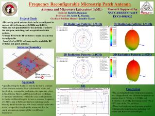
Proposed Design Criteria • Patch antenna on microstrip board • 2 GPS application frequencies • 1.227 GHz • 1.575 GHz • Double stub impedance matching network • Matched to 50Ω • MEMS preferred switching method
Patch Antenna • Rogers Corporation RO3010 Microstrip Board • εr = 10.2, h = 5 mils • 1.227 GHz, 1.575 GHz • Right Hand CircularPolarization
Patch Antenna • Equations: • L1 = W = 2.988 cm • L2 (total) = 3.795 cm • dL2 = 0.807 cm
Switching Method • MEMS Switch • RMSW201, RADANT MEMS • SPST • DC to 20 GHz • 0.3dB Insertion Loss @ 2GHz • 35dB Isolation Loss @ 2GHz • 1.9mm x 1.85mm package size • +/- 90V Gate-Source Voltage • Wire bonding to board
Switching Method • DC-DC Converter: +5V to -90V
Implementing MEMS • Via holes to ground plane
Implementing MEMS • Conductive epoxy over via hole • Wire bonding, gold plating
Simulations: Linear Patch Antenna • PCAAD 6.0 • Simulate Linear Patch Antenna (square or rectangle) to determine resonant frequency • Simulate both patches separately before integration into one system
Simulations: Polarized Patch Antenna • Sonnet or Momentum • Right Hand Circular Polarization • Modify linear patch antenna design to truncate corners.
Simulations: Include Switches • Patches connected or not connected
Double Stub Matching Network • A matching network allows maximum power transfer • Useable for most load admittances
Double Stub Matching Network • Reconfigurable to match different patch resonant frequencies • Can not be analyzed until patch antenna system is designed • Methods: • Using Smith Charts: • Cancel out all imaginary impedances • Match impedance to 50Ω • Must be done for each patch (Reconfigurable)
Task Schedule • Research (completed) • Antenna Type • Switching Device • Polarization Methods • Simulations (in progress) • Linear Patch Antenna • 1.575 GHz, 1.227 GHz • Polarized Patch Antenna • Determine Switch Parameters • Polarized Patch Antenna w/ switches (on/off)
Task Schedule (cont.) • Impedance Matching – Double Stub • Smith Chart • Stub Lengths • Open or Short Circuit • Board Fabrication • Microstrip Board • Implement MEMS • Switching Device
Task Schedule (cont.) • Analysis • Resonant Frequencies • Efficiency • Comparison to Simulation Results
Tentative Remaining Schedule • Simulations – Purchasing of Parts • Complete by end of Fall ’11 Semester • Impedance Matching • Weeks 1-2 • Fabrication • Weeks 3-10 • Analysis • Weeks 11-15