Download
1 / 1
10 likes | 151 Views
Integration of Laser-Welded Ag Nanowire Transparent Conducting Layers on Photovoltaic Devices (DMR-0819860 ) IRG-B: C. B. Arnold, A. Kahn and J. Sturm Princeton Center for Complex Materials (PCCM).

E N D
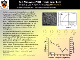
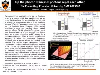
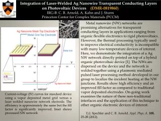
Integration of Laser-Welded Ag Nanowire Transparent Conducting Layers on Photovoltaic Devices (DMR-0819860) IRG-B: C. B. Arnold, A. Kahn and J. Sturm Princeton Center for Complex Materials (PCCM) Metal nanowire (NW) networks are promising alternatives for transparent conducting layers in applications ranging from organic flexible electronics to rigid photovoltaics. However, the thermal processing typically used to improve electrical conductivity is incompatible with many low-temperature devices of interest. Here, we demonstrate the integration of a Ag NW network directly printed on top of a hybrid organic photovoltaic device [1]. The NWs are dispersed on the device and the network is welded together using a plasmonic mediated pulsed laser processing method developed in our group to localize the incident heating at the NW junctions. Results show high efficiency and an improved fill factor as compared to traditional vapor deposited electrodes. On-going work examines the nature of these non-traditional interfaces and the application of this technique to other organic electronic devices of interest. 1) J. Spechler and C. B. Arnold. Appl. Phys. A.108, 25-28(2012). Current-voltage (IV) curves for standard device using a vapor deposited metal grid versus a laser welded nanowire network electrode. The efficiency is approximately the same but the fill factor is significantly improved. Inset shows processed NW network