Download
1 / 2
20 likes | 156 Views
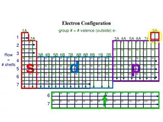
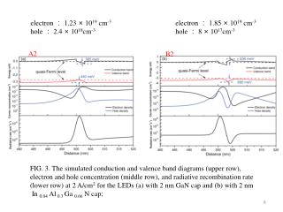
electron : 1.23 × 10 19 cm -3 hole : 2.4 × 10 18 cm -3. electron : 1.85 × 10 19 cm -3 hole : 8 × 10 17 cm -3. A2. B2. FIG. 3. The simulated conduction and valence band diagrams (upper row), electron and hole concentration (middle row), and radiative recombination rate

E N D
electron : 1.23 × 1019 cm-3 hole : 2.4 × 1018cm-3 electron : 1.85 × 1019 cm-3 hole : 8 × 1017cm-3 A2 B2 FIG. 3. The simulated conduction and valence band diagrams (upper row), electron and hole concentration (middle row), and radiative recombination rate (lower row) at 2 A/cm2 for the LEDs (a) with 2 nm GaN cap and (b) with 2 nm In 0.04 Al 0.3 Ga 0.66 N cap;
61% 54% B1 B2 B0 B3 1.6 10 (c) the simulated internal quantum efficiency (IQE) as a function of current density.