Download
1 / 13
650 likes | 1.87k Views
HIGH PRODUCTIVITY 300mm HDP-CVD FOR NEXT-GENERATION GAP FILL PROCESSES. Paper Authors : Paddy Krishnaraj, Bruno Geoffrion, et al. Applied Materials. * Material in this presentation in mainly covered from 3 reference papers by researchers Nyugen and Cote, Watson Labs - IBM.

E N D
HIGH PRODUCTIVITY 300mm HDP-CVD FOR NEXT-GENERATION GAP FILL PROCESSES Paper Authors : Paddy Krishnaraj, Bruno Geoffrion, et al. Applied Materials * Material in this presentation in mainly covered from 3 reference papers by researchers Nyugen and Cote, Watson Labs - IBM Presented as a review for ELEC 7730 course by Nikhil Mehta, Auburn University
Need for this paper • The industry shift to 300mm wafers • Device size shrinkage by 20-30% with nearly 30% increase in overall efficiency annually • Need for gap filling processes for <0.1 micron (nm) level • Fewer process steps for low cost in fabrication
Why HDP-CVD ? • Produce dielectric layers with minimal (controlled) substrate heating • No deleterious effect on underlying oxide or gate structures • Suitable for filling sub half μ gaps with high aspect ratio • Require fewer step to reduce overall cost
HDP-CVD Fig Top : Applied Materials Fig Bottom and Specs: Paper: HDP CVD deposition for ICs - S. V. Nguyen –IBM Watson Labs.
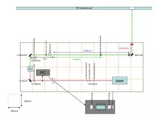
Apply RF current in the coil • Generate RF magnetic field around the coil • Induce RF electric field in the chamber • Heating of electrons, formation of electron energy distribution • Gas ionization, gas phase reactions • Surface reactions, recombination of ions and electrons at the walls, sputtering, deposition, etching • Sheath formation CFDRC – Virtual Reactor Equipment simulator, ICP Plasma Analysis with CFD
Basic terms and their importance • Deposition/Sputtering rate ratio (D/S) • if too small – corners of the features to be filled sputters off • if too large – voids or weak seams can form • Precursor composition • System to be kept continuously at low pressure • Simple reactants like Silane / SiF4 / O2 used Paper - Plasma-assisted CVD of dielectric thin films for ULSI semiconductor circuits – Cote et al., IBM Watson Labs
HDP-CVD films properties as a function of different parameters Parameter ↑ At% F Stress Uniformity Stability (stress) SiF4 flow ↑ ↓ - - SiF4 / SiH4 ratio ↑ ↓ ↓ ↑ Temperature ↓ ↓ - ↓ Bias rf power ↓ ↓↑ ↓ Source rf power ↓ ↓↑ Mixed Paper - Plasma-assisted CVD of dielectric thin films for ULSI semiconductor circuits – Cote et al., IBM Watson Labs
Characteristics of HDP-CVD growth film Paper: HDP CVD deposition for ICs - S. V. Nguyen –IBM Watson Labs.
Characteristics of HDP-CVD growth film Paper: HDP CVD deposition for ICs - S. V. Nguyen –IBM Watson Labs.
HDP CVD Gap Fill Processes Needed for • Interlevel dielectric (ILD) • Gap fill for gate conductors • Gap fill for shallow trench isolation (STI) - Integration problem - Aspect ratio, deposition parameters, dimensions of the gap fill structures affect the amount of material to be deposited. D/S value of a process does not remain constant during deposition - Need for advanced simulation for a particular geometry prior to deposition
HDP-CVD –Gap Fill Applications • The need void free gap fill for high aspect ratio structures in ICs Paper: HDP CVD deposition for ICs - S. V. Nguyen –IBM Watson Labs.
D/S important parameter in gap fill processes * • D/S ratio of 3.0 - 3.5 for aspect ratio 2-2.5 of 0.25-0.18 μ structures • D/S ratio of > 3.5 for aspect ratio > 3 for sub 0.1 μ structures * Paper: HDP CVD deposition for ICs - S. V. Nguyen –IBM Watson Labs. Source : IBM watson labs and Applied Materials
References • Plasma-assisted CVD of dielectric thin films for ULSI semiconductor circuits – D.R. Cote et al., Watson Labs – IBM Journal • HDP-CVD of silicon based dielectric films for Integrated circuits – S.V. Nyugen, Watson Labs – IBM Journal