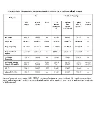
Semiconductor Diodes and Their Applications - Introduction and Semiconductor Materials
120 likes | 137 Views
This text provides an introduction to semiconductor diodes and their applications. It covers semiconductor materials, energy levels, extrinsic materials, and more. References from reputable textbooks are included.

Semiconductor Diodes and Their Applications - Introduction and Semiconductor Materials
E N D
Presentation Transcript
Ministry of teaching& high education Al- Mustansiriya University College of engineering Computer & Software engineering 1' class Electronic 1 Electronic I • References: • 1. Electronic Devices and Circuit theory By: Robert L, Boylested & Nashelsky • 2. Millman & Halikas “ Electronic Devices & Circuits” • 3. Jacob Millman & Arvin Grabel “Microelectronics” • 4. Jimmie J.”Electronic Devices & Circuits” • Contents: • Semiconductor Diodes Chapter 1 • Diode Applications Chapter 2 • Bipolar Junction Transistors Chapter 3 • DC Biasing – BJTs Chapter 4 • BJT Smalll- signal Analysis Chapter 5
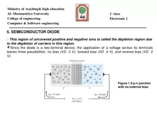
Chapter One Semicoductor Diodes 1.1 Introduction 1.2 Semiconductor Materials :Ge , Si , Ga As 1.3 Energy Levels 1.4 Extrinsic Materials—n- and p-Type 1.5 Semiconductor Diode 1.6 Ideal Versus practical 1.7 Diode Equivalent Circuits 1.8 Transition and Diffusion Capacitance 1.9 Reverse Recovery Time 1.10 Zener Diodes 1.15 Light-Emitting Diodes (LEDs) & other types of diodes
1. Semiconductor Diodes • The miniaturization that has resulted leaves us to wonder about its limits. • Complete systems now appear on wafers thousands of times smaller than the single element of earlier networks. • The first integrated circuit (IC) working at Texas instrument in 1958 • Today, the intel pentium 4 processor has more than 42 million transistors. • The first device to be introduced here is the simplest of all electronic devices, yet has a range of applications that seems endless. • 2. Semiconductor Materials :Ge , Si , Ga As : • The term conductor is applied to any material that will support a generous • flow of charge when a voltage source of limited magnitude is applied across • its terminals. • An insulator is a material that offers a very low level of conductivity under • pressure from an applied voltage source. • A semiconductor, therefore, is a material that has a conductivity level somewhere between the extremes of an insulator and a conductor. • As indicated by Fig. 1a, the germanium atom has 32 orbiting electrons, while • silicon has 14 orbiting electrons. In each case, there are 4 electrons in the outermost(valence) shell.
The potential (ionization potential) required to remove any one of • these 4 valence electrons is lower than that required for any other electron in the structure. • In a pure germanium or silicon crystal these 4 valence electrons are bonded to • 4 adjoining atoms, as shown in Fig. 2 for silicon. Both Ge and Si are referred to as tetravalent atoms because they each have four valence electrons. • A bonding of atoms, strengthened by the sharing of electrons, is called covalent bonding Figure 1 Atomic structure: (a) germanium; (b) silicon. Figure 2 Covalent bonding of the silicon Atom
Intrinsic materials are those semiconductors that have been carefully refined • to reduce the impurities to a very low level—essentially as pure as can be • made available through modern technology. • An increase in temperature of a semiconductor can result in a substantial increase in the number of free electrons in the material. • Semiconductor materials such as Ge and Si that show a reduction in resistance with increase in temperature are said to have a negative temperature coefficient. • ENERGY LEVELS: • In the isolated atomic structure there are discrete (individual) energy levels associated with each orbiting electron, as shown in Fig. 3a. Each material will, in fact, have its own set of permissible energy levels for the electrons in its atomic structure. • The more distant the electron from the nucleus, the higher the energy state, and any electron that has left its parent atom has a higher energy state than any electron in the atomic structure.
Figure 3 Energy levels: (a) discrete levels in isolated atomic structures; (b) conduction and valence bands of an insulator, semiconductor, and conductor.
The net result is an expansion of the discrete levels of possible energy states for the valence electrons to that of bands as shown in Fig. 3b. Note that there are boundary levels and maximum energy states in which any electron in the atomic lattice can find itself, and there remains a forbidden region between the valence band and the ionization level. 4. EXTRINSIC MATERIALS— n- AND p-TYPE • A semiconductor material that has been subjected to the doping process is called an extrinsic material. • There are two extrinsic materials of immeasurable importance to semiconductor • device fabrication: n-type and p-type. Each will be described in some detail in the • following paragraphs. 4.1 n-Type Material Both the n- and p-type materials are formed by adding a predetermined number of impurity atoms into a germanium or silicon base. The n-type is created by introducing those impurity elements that have five valence electrons (pentavalent), such as antimony, arsenic, and phosphorus. The effect of such impurity elements is indicated in Fig. 4 (using antimony as the impurity in a silicon base). Note that the four covalent bonds are still present. There is, however, an additional fifth electron due to the impurity atom, which is unassociated with any particular covalent bond.
Figure 4 Antimony impurity in n-type material • Diffused impurities with five valence electrons are called donor atoms. • The effect of this doping process on the relative conductivity can best be described • through the use of the energy-band diagram of Fig. 5. Note that a discrete energy level (called the donor level) appears in the forbidden band with an Eg significantly less than that of the intrinsic material.
Figure 5 Effect of donor impurities on the energy band structure. 4.2 p-Type Material • The p-type material is formed by doping a pure germanium or silicon crystal with impurity atoms having three valence electrons. The elements most frequently used for this purpose are boron, gallium, and indium. The effect of one of these elements,boron, on a base of silicon is indicated in Fig. 6
Figure 6 Boron impurity in p-type material. • The diffused impurities with three valence electrons are called acceptor atoms.
4.3 Electron versus Hole Flow • The effect of the hole on conduction is shown in Fig. 7. If a valence electron acquires sufficient kinetic energy to break its covalent bond and fills the void created • by a hole, then a vacancy, or hole, will be created in the covalent bond that released • the electron. Figure 7 Electron versus hole flow. 4.4 Majority and Minority Carriers • In an n-type material (Fig. 1.8a) the electron is called the majority carrier • and the hole the minority carrier. • For the p-type material the number of holes far outweighs the number of electrons, as shown in Fig. 1.8b. Therefore: • In a p-type material the hole is the majority carrier and the electron is the • minority carrier.