Diode Circuits
Diode Circuits. Voltage Regulation. Rectifier Circuit. c03f34. Half-Wave Rectifier. T in. Cause of ripple: the capacitor is discharged for almost an entire period. c03f36. inversion. Ripple Reduction: Do not allow the capacitor to discharge so frequently.


Diode Circuits
E N D
Presentation Transcript
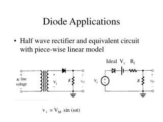
Voltage Regulation Rectifier Circuit
c03f34 Half-Wave Rectifier Tin Cause of ripple: the capacitor is discharged for almost an entire period.
c03f36 inversion Ripple Reduction: Do not allow the capacitor to discharge so frequently
An Inverting Half-Wave Rectifier If Vin >0, D1 and D2 are off. If Vin <0, D1 and D2 are on and Vout>0.
An Non-Inverting Half-Wave Rectifier If Vin >0, D1 and D2 are on, Vout>0. If Vin <0, D1 and D2 are off.
Full-Wave Rectifier Inverting Non-Inverting
Full-Wave Rectifier Alternative Drawing Full-Wave A.K.A. Bridge Rectifier Non-Inverting Inverting
Using Constant Voltage Diode Model Vout=-Vin-2VD, on Vout=Vin-2VD, on
Input versus Output |Vin|<2VD,on
Modification of Ripple Estimation Formula • Modification: • Turn-on voltage • 1/2 to account for inversion of negative • peaks.
Maximum Reverse Voltage VB=VD,on Vp is the amplitude of Vin VA=VP VAB=VP-VD,on Maximum reverse voltage is approximately Vp
Compare Maximum Reverse Bias Voltage to Half-Wave Rectifier A reverse diode voltage must sustain larger reverse bias voltage
Application of Limiting Circuits Limit the signal amplitude at a suitable point in the receiver
Application of Voltage Doubler Electronic systems typically provide a global supply voltage: 3V Design of some circuits will be simplified if they from a higher supply voltage.
Voltage Doubler Floating Capacitor Capacitor Divider
Capacitor Diode Circuit Ideal diode. Vout pinned to 0 V Positive charges begin to leave the left Plate of C1, turning D1 off. C1 is now a floating capacitor
Voltage Doubler 0 to 2Vp waveform Peak Detector
Diode as a Voltage Shifter Application: We may need to shift the average level of a signal up and down because the subsequent stage (e.g. an amplifier) may not operate properly with the present dc level.
A simple electronic switch CK is 1: I1=1, diodes are shorted, and Vin=Vout. CK is 0,diodes are off, charges are stored across C1.