Download
1 / 31
380 likes | 595 Views
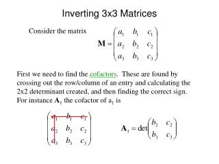
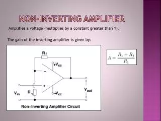
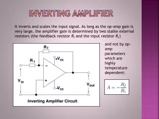
Experiment 11: An Inverting Amplifier. Circuit Diagram for Inverting Amplifier. Op Amp Equivalent Circuit. v d = v 2 – v 1 A is the open-loop voltage gain. v 2. v 1. An op amp can be simulated as a voltage controlled voltage source. Typical Op Amp Parameters.

E N D
Op Amp Equivalent Circuit vd = v2 – v1 A is the open-loop voltage gain. v2 v1 An op amp can be simulated as a voltage controlled voltage source.
DC Voltage Transfer Characteristic Positive Saturation Region Negative Saturation Region
PSpice Simulation • Transient Analysis • Output plot mimics the oscilloscope display. • Select Vsin • Vsin is a sinusoidal voltage source. • Do NOT use Vac as the sinusoidal voltage source. • This source should be used when running an AC Sweep simulation.
Setting Attributes for Vsin: Schematics For a simple sinusoid, set: VOFF (a d.c. offset voltage) to 0V, VAMPL (the amplitude of the sine wave) to the appropriate value, FREQ (frequency in Hertz – this is not angular frequency) to the appropriate value.
Setting Attributes on Vsin:Capture • Double click on the labels (VOFF, VAMPL, and FREQ) individually in schematics and change their value in the pop-up window that opens.
Setting Attributes on Vsin:Capture • Or, click on the symbol for Vsin and change the values for the attributes in the Property Editor pop-up window. • FREQ is at the left side, VOFF and VAMPL are at the far right side. Scroll right to find VOFF and VAMPL
Simulation Set-up:Schematics Final Time should be 3-5 times the period (T) of V1. T = 1/f where f is the frequency of the sinusoidal signal.
To obtain a smoother sinusoid In the Transient pop-up window, set a Step Ceiling that is a small fraction of the period of the sinusoid that you are plotting.
Place voltage markers at Vsin and the output pin of the operational amplifier.
Plot of the input voltage and output voltage as a function of time You can use
Cursors • Click on the plot to activate the cursors and move them along the plot that has been selected. • The voltage and time of the point on the curve where the cursor is located is displayed in the Probe Cursor pop-up window. • Click on the symbol next to the plot name to change which plot the cursors are associated with.
LM 324 Quad Op Amp http://www.national.com/ds/LM/LM124.pdf
The Notch The recessed “U” on the DIP (dual inline package) package should be matched with the image when looking down at the package after it has been inserted into the breadboard.
LM 324 Quad Op Amp • GND is actually V-. • If you wire V+ and V- backwards, the dip package will be come very hot – so hot that it will melt the plastic breadboard beneath it. • If you smell ‘hot plastic’, pull the power plug out. • Wait until the chip cools down before removing it from the ANDY board. • The chip is probably damaged, replace it rather than reusing it. • Integrated chips (ICs) can be damaged by electrostatic discharge (ESD). • It is always a good idea to ground yourself before touching an IC (e.g., touch something metallic).
Input Voltage Source • Use the sine wave generator on the Velleman scope. • Set the amplitude of the sine wave to 5V • Note that the amplitude on the Velleman scope is actually peak-to-peak so you should actually set the amplitude to 10V on the function generator. • Set the frequency of the sine wave to 1000Hz. • Connect BNC cable to function generator (bottom BNC connection). • Clip red probe to end of R1. • Clip black probe (ground) to end of R2 or R3.
Voltage Measurements using Oscilloscope • Channel 1: • Red probe placed between function generator and R1. • Black probe connected to same point as the black wire from the function generator. • Channel 2: • Red probe placed between output of the LM 324 and the feedback resistor, Rf, or between output of the LM 324 and R3. • Black probe connected to same point as the black wire from the function generator.
Measurements 1. As suggested in lab manual, set trim pot value such that the output voltage of the op amp is equal to -2.0V when the input voltage is +1.0V. • Take a screen shot of the input and output voltage as a function of time, displaying at least 3 cycles. • Remove Rf from the circuit. Measure and record the resistance between pins 1 and 2. • Measure the output voltage at the following input voltages: • 0V, +/-1V, +/-2V, +/-3V, +/- 4V, and +/-5V. • use cursors in scope program • Plot the output voltage as a function of the input voltage. • Determine • the gain of the inverting amplifier in the linear region of the voltage transfer characteristic using a least squares determination of the slope in the linear region • the output voltage at the positive and negative saturation regions.
Measurements 2. Set trim pot value such that the output voltage of the op amp is equal to -3V when the input voltage is +1.0V. • Take a screen shot of the input and output voltage as a function of time, displaying at least 3 cycles. • Remove Rf from the circuit. Measure and record the resistance between pins 1 and 2. • Measure the output voltage at the following input voltages: • 0V, +/-1V, +/-2V, +/-3V, +/- 4V, and +/-5V. • use cursors in scope program • Plot the output voltage as a function of the input voltage. • Determine • the gain of the inverting amplifier in the linear region of the voltage transfer characteristic using a least squares determination of the slope in the linear region • the output voltage at the positive and negative saturation regions.
Measurements 3. Set trim pot value such that the output voltage of the op amp is equal to -4V when the input voltage is +1.0V. • Take a screen shot of the input and output voltage as a function of time, displaying at least 3 cycles. • Remove Rf from the circuit. Measure and record the resistance between pins 1 and 2. • Measure the output voltage at the following input voltages: • 0V, +/-1V, +/-2V, +/-3V, +/- 4V, and +/-5V. • use cursors in scope program • Plot the output voltage as a function of the input voltage. • Determine • the gain of the inverting amplifier in the linear region of the voltage transfer characteristic using a least squares determination of the slope in the linear region • the output voltage at the positive and negative saturation regions.
Measurements • Measure exact values of V+ and V- powering the LM 324 op amp.
Discussion Section • Compare the gains found in Analysis Section and the measured results. • Explain any discrepancies • Explain the major differences between the PSpice simulation and the measurements of the output voltage as a function of time. • Compare the averaged positive and negative saturation voltages with the measured values of the power supplies. • Does the saturation voltage depend on the amplifier gain (within experimental error)? • Does the saturation voltage agree with that specified in the LM 324 data sheet (find on-line)?