Download
1 / 25
250 likes | 403 Views
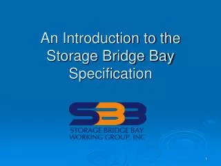
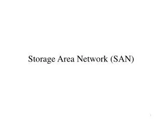
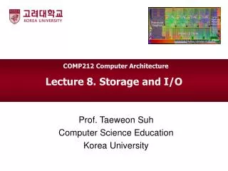
COMP212 Computer Architecture. Lecture 8. Storage and I/O. Prof. Taeweon Suh Computer Science Education Korea University. A Computer System. CPU. Main Memory (DDR2). FSB (Front-Side Bus). North Bridge. Graphics card. DMI (Direct Media I/F). I/O devices. South Bridge. Hard disk.

E N D
COMP212 Computer Architecture Lecture 8. Storage and I/O Prof. Taeweon Suh Computer Science Education Korea University
A Computer System CPU Main Memory (DDR2) FSB (Front-Side Bus) North Bridge Graphics card DMI (Direct Media I/F) I/O devices South Bridge Hard disk USB PCIe card But, don’t forget the big picture!
Disk Storage • Disk (typically HDD) provides a non-volatile, long-term storage • It is located at the lowest level in the memory hierarchy • Magnetic disk • A rotating platter is coated with magnetic material • Use a movable head to access the disk for read/write arm arm head platters
Magnetic Disk Structure • Magnetic disk has a collection of platters • Each platter has 2 recordable disk surfaces • The stack of platters is rotated at 5400 to 15,000 RPM (Revolutions Per Minute) • The diameter of platters is from 1-inch to just over 3.6 inches • Each platter surface is divided into concentric circles, called tracks • There are typically 10,000 ~ 50,000 tracks per surface • Each track is, in turn, divided into sectors that contain information • Each track may have 100 ~ 500 sectors • Each sector stores typically 512 bytes Sector Track platters
Magnetic Disk Characteristic • The disk access (read or write) involves the following steps • Seek: position head over the proper track • Seek time: time to position the head over the proper track • Average seek time is usually advertized as 3ms ~ 13ms • Rotation: rotate platter to position the desired section under the head • Rotation latency: time to position the head over the desired sector • Average rotation latency = (0.5 rotation/5,400RPM = 5.6ms) ~ (0.5 rotation/15,000RPM = 2.0ms)
Magnetic Disk Characteristic (Cont) • Transfer: transfer a block of bits (1 or more sectors) to the disk controller’s cache • 70 to 125 MB/s are typical disk transfer rates in 2008 • The disk controller’s “cache” takes advantage of spatial locality in disk accesses • Cache transfer rates are much faster (e.g., 375 MB/s) • Controller overhead: the overhead the disk controller imposes in performing a disk I/O access • Disk access time = seek time + rotation latency + transfer time + controller overhead Hard-disk cache (or buffer)
Example • What is the average time to read or write a 512B sector for a typical disk rotating at 15,000RPM? • Avg. seek time = 4ms • Transfer rate = 100MB/sec • Controller overhead = 0.2ms • Disk access time = avg. seek time + avg. rotation latency + transfer time + controller overhead • Avg. seek time = 4 ms • Avg. rotation latency = (0.5 rotation/15,000RPM) = 2ms • Transfer time = 512B / (100MB/sec) = 0.005 ms • Controller overhead = 0.2 ms • Disk access time = 4ms + 2ms + 0.005ms + 0.2 ms = 6.2 ms • Rotation latency is often the largest component of access time!
Disk Interface Standards • ATA (Advanced Technology Attachment) • Evolved from IDE (Integrated Drive Electronics) standard • Parallel ATA: Interface standard for the connection of storage devices such as hard disks, solid-state drives, and CD-ROM drives in computers • Serial ATA (SATA) offers faster and more efficient data transfer compared to PATA. SATA has mostly replaced PATA in PCs • SCSI (Small Computer Systems Interface) • Pronounced “skuzzy” • Used for hard disks and tape drives PATA Interface SATA Interface SCSI Connectors
Flash Storage • Flash memory is the first credible challenger to disks • Flash memory is semiconductor memory (like DRAM and SRAM) that is nonvolatile like disks • Flash memory has latency 100 to 1000 times faster than disk and is smaller, more power efficient, and more shock resistant • In 2008, the price of flash is $4 to $10 per GB • About 2 to 10 times higher than disk • About 5 to 10 times lower than DRAM 250 GB SSD (Solid State Drive) floating gate transistor
Flash Types • NOR flash: bit cell like a NOR gate • Random read/write access • Used for BIOS memory • NAND flash: bit cell like a NAND gate • Denser (bits/area) • Cheaper per GB • Read is on a page basis (page is typically 512B, 2048B or 4096B) • Used for USB keys and SSDs • Limitations of Flash memory • Erasure on a block basis (typical block sizes are 64KB, 128KB, or 256KB) • Erasing means setting all bits in a block to 1 • Flash bits wears out after 100,000 accesses for NOR flash and after 10,000~100,000 accesses for NAND flash • Wear leveling: hardware controller remaps data to less used blocks
A Computer System CPU Main Memory (DDR2) FSB (Front-Side Bus) North Bridge Graphics card DMI (Direct Media I/F) I/O devices South Bridge Hard disk USB PCIe card
A Typical I/O System Schematic (Simplified) Interrupts CPU Core Cache bus Memory Bus, I/O bus Memory Controller I/O Controller I/O Controller I/O Controller Main Memory Graphics Card Network Disk Disk
I/O Interconnection • A bus is a shared communication link • A single set of wires used to connect multiple components • Composed of address bus, data bus, and control bus (read/write) • Advantages • Versatile – new devices can be added easily and can be moved between computer systems that use the same bus standard • Low cost – a single set of wires is shared in multiple ways • Disadvantages • Communication bottleneck – bus bandwidth limits the maximum I/O throughput • The maximum bus speed is largely limited by • The length of the bus • The number of devices on the bus
I/O Interconnection (Cont) • I/O devices and interconnection largely contribute to the performance of computer system • Traditionally, parallel shared wires had (have) been used to connect I/O devices • As the clock frequency increases for communicating with I/O devices, parallel shared wires suffer from clock skew and interference among wires • Industry transitioned from parallel shared buses to high-speed serial point-to-point interconnections
Types of Buses • Processor-memory bus • Front Side Bus (FSB), proprietary bus • Replaced by QPI (QuickPath Interconnect) in Intel • Replaced by Hypertransport in AMD • Short and high speed • Matched to the memory system to maximize the memory-processor bandwidth • Optimized for cache block transfers • Backplane (backbone) bus • Industry standard • e.g., PCIexpress • Allow processor, memory and I/O devices to coexist on a single bus • Used as an intermediary bus connecting I/O busses to the processor-memory bus • I/O bus • Industry standard • e.g., SATA, USB, Firewire • Usually is lengthy and slower • Needs to accommodate a wide range of I/O devices Processor-memory bus Backplane bus CPU Main Memory (DDR2) FSB (Front-Side Bus) North Bridge Graphics card DMI (Direct Media I/F) South Bridge Hard disk USB I/O bus
How Does CPU Access I/O Devices? • All the I/O devices have registers implemented, so software programmers can use them to control the devices • Then, for programming, where and how to write to or read from? • There are 2 ways to access I/O devices • Memory-mapped I/O • I/O-mapped I/O • Memory-mapped I/O • I/O device is mapped to a memory space • CPU generates a memory transaction to access I/O device • To access I/O device • In MIPS, use lwor sw instructions • In x86, use mov instruction Memory Space 0xFFFF_FFFF (4GB-1) I/O device I/O device I/O device 0x3FFF_FFFF (1GB-1) Main Memory (1GB) 0x0
How CPU Accesses I/O Devices? • I/O-mapped I/O • I/O devices are mapped to I/O space • CPU generates I/O transaction to access I/O device • To access I/O device • In x86, there are in and out instructions. • In x86, I/O space is 64KB • To differentiate memory space and I/O space, there should be hardware support • ISA support • In x86, mov instruction for memory transaction and in,outinstruction for I/O transaction • Physical pin from processor indicating the transaction type (memory or I/O) • For example, the pin is driven to “1” for memory transaction or “0” for I/O transaction I/O Space (64KB in x86) 0xFFFF (64KB-1) I/O device I/O device I/O device 0x0
How I/O Communicates with CPU? • Polling • CPU periodically checks the status of I/O devices to determine its need for service • CPU is totally in control • Can waste a lot of CPU time due to speed differences • Interrupt • I/O device issues an interrupt to indicate that it needs attention • An I/O interrupt is asynchronouswrt (with respect to) instruction execution • It is not associated with any instruction, so doesn’t prevent any instruction from completing • You can pick your own convenient point in the pipeline to handle the interrupt
DMA (Direct Memory Access) • Typically, moving data from one place to another involve CPU instructions • Load (lw) from a location (e.g. memory in an I/O device) • Store (sw) to another location (e.g. main memory) • Moving a large chunk of data with CPU instructions could take a large fraction of CPU time • DMA has the ability to transfer large blocks of data directly to/from the memory without involving the processor • The processor initiates the DMA transfer by supplying source and destination addresses, the number of bytes to transfer • The DMA controller manages the entire transfer (possibly thousand of bytes in length), arbitrating for the bus • When the DMA transfer is complete, the DMA controller interrupts the processor to inform that the transfer is complete • There may be multiple DMA devices in one system • Processor and DMA controllers contend for bus cycles and for memory
Concluding Remarks • That’s it! Folks • I hope you have enjoyed (?) this class • If you think that you successfully finished the course, you should have confidence in computers now! • But, you just have laid the foundations for the further study of computer science and engineering
Read/Write Block Diagram of Memory • An M-bit data value can be read or written at each unique N-bit address N-bit address lines Memory • Example: Byte-addressable 2MB memory • M = 8 (because of byte-addressability) • N = 21 (1 word = 8-bit) N 2N words (M-bit per word) Chip Select (Chip Enable) M M-bit Data Output (for Read/Write) Modified from Prof Sean Lee’s Slide, Georgia Tech
1-bit 1-bit 1-bit 1-bit 1-bit 1-bit 1-bit 1-bit 1-bit 1-bit 1-bit 1-bit 1-bit 1-bit 1-bit 1-bit 1-bit 1-bit 1-bit 1-bit 1-bit 1-bit 1-bit 1-bit 1-bit 1-bit 1-bit 1-bit 1-bit 1-bit 1-bit 1-bit Memory Organization Example 4 words x 8 bits Wordline (WL) 2-to-4 Decoder 0 1 A0 2 A1 3 CS BitLine D6 D4 D2 D0 D7 D5 D3 D1 Chip Select Modified from Prof Sean Lee’s Slide, Georgia Tech
1-bit 1-bit 1-bit 1-bit 1-bit 1-bit 1-bit 1-bit 1-bit 1-bit 1-bit 1-bit 1-bit 1-bit 1-bit 1-bit 1-bit 1-bit 1-bit 1-bit 1-bit 1-bit 1-bit 1-bit How to Address Memory 4 words x 8 bits 2-to-4 Decoder 0 A0=1 1 1-bit 1-bit 1-bit 1-bit 1-bit 1-bit 1-bit 1-bit 2 A1=0 3 CS D6 D4 D2 D0 D7 D5 D3 D1 Chip Select=1 Access address = 0x1 Modified from Prof Sean Lee’s Slide, Georgia Tech