Efficient Module Assembly Process for Pixel Sensors
180 likes | 199 Views
Detailed overview of assembly flow, individual pieces, production plans, rates, cost summary, and development plans for assembling pixel modules. Includes key insights on bump bonding, wafer thinning, die probing, and mechanical assembly.

Efficient Module Assembly Process for Pixel Sensors
E N D
Presentation Transcript
Module AssemblyWBS 1.1.1.5 • Pixel module anatomy • Assembly Flow • Individual pieces • Production Plan and Rates • Cost and Schedule Summary • Development plans M. Garcia-Sciveres - ATLAS Pixel Review - Module Assembly
The Pixel Module pigtail Sensor beyond ASICs Flex Hybrid & Pigtail Bumps Wirebonds Schematic Cross Section (through here) Perspective View M. Garcia-Sciveres - ATLAS Pixel Review - Module Assembly
FE IC Wafers and Die • US to thin and probe wafers • US to return Known Good Die (KGD) to bump vendors When Do We Probe Wafers/Die? • During development: after fab, bumping, thinning & dicing. • After all yields are known can select best stage(s) • Same setup used at all stages. • Bumped wafers must be probabed (=> resist openings) • Use CDF method for single die probing. M. Garcia-Sciveres - ATLAS Pixel Review - Module Assembly
Bump Bonding • Bump Bonding is a non-US responsibility. • Includes deposition of bumps/under bump metalization on FE IC/sensor wafers as well as flip chip assembly. • STATUS: • Two vendors qualified via dummy and active prototypes (small qtty) • Both have handled 4” sensor and 6” IC wafers. • They have or are acquiring 8” wafer capability. • IZM and AMS to produce 2x50 dummy modules in 2001(mechanically identical to production modules) • Active modules to be produced in 2001 as FE IC availability permits. • Third vendor being considered (only has 6” wafer capability => DMILL FE ICs). • Projected production rate 40 modules/wk (20 IZM + 20 AMS). AMS (IT) – evaporative indium IZM (GER) – solder bumps Sofradir– reflowed indium M. Garcia-Sciveres - ATLAS Pixel Review - Module Assembly
FE IC Wafer With Bumps M. Garcia-Sciveres - ATLAS Pixel Review - Module Assembly
IC Wafer Thinning • Thinning of all IC wafers is a US responsibility. • FE IC wafers are back-ground to reduce material and fit envelope. • Final thickness 150mm (goal) to 300mm (current envelope limit). • 6” Wafers processed by AMS have been thinned to 150-175mmand thinned die have been used to build active modules. • 6” Wafers processed by IZM have been thinned to 200mm. Limitations understood and dummy wafers are in preparationwith modifications to the protective photoresist application. • All grinding done at Okamoto, San Jose (automated facility). • Investigating possibility of European vendor as second source and to reduce shipping of IC wafers. • 8” wafer thinning to be explored. 300mm may be the limit. M. Garcia-Sciveres - ATLAS Pixel Review - Module Assembly
Single Die Probing Fixture used to Probe 8,000 SVX3D chips for CDF CDF Chip Probing Results M. Garcia-Sciveres - ATLAS Pixel Review - Module Assembly
Bare Modules • US to probe and accept for module assembly. • Prepare to debug modules that fail probe. • Must know identity of each die (marking under study). • Assume returning to bump vendor or elsewhere for die replacement. Back sides of 16 FE ICs Detector barely visible M. Garcia-Sciveres - ATLAS Pixel Review - Module Assembly
Flex Hybrid and Pigtail(Covered in separate presentation) • US to fabricate all flex hybrids and load passives. • US to share MCC loading and test. • US to fabricate and test all disk pigtails. • Flex hybrid is universal up to module assembly. • Customized for specific disk by adding pigtail before module assembly. • Flex with pigtail must be Known Good Part. (tested all connections, MCC function, HV paths) M. Garcia-Sciveres - ATLAS Pixel Review - Module Assembly
Mechanical Assembly • Prototype fixtures designed, built and tested M. Garcia-Sciveres - ATLAS Pixel Review - Module Assembly
Assembly of Modules onto Sectors • Same base assembly as Module fixture. • Prototyping advanced: techniques used to test prototype sectors. Carbon sector structure Thermal compound for FE chips on module M. Garcia-Sciveres - ATLAS Pixel Review - Module Assembly
US Production Sites • Wafer/Die Probing: LBNL • Wafer thinning: Okamoto (Bay Area) • Wafer dicing: various qualified vendors (Bay Area) • Die sort and mark: LBNL • Bare module probing: LBNL • Flex Hybrid Fab:Compunetics-type vendors TBD, CERN. • Flex Hybrid assembly: Flex One, SMD, etc., Oklahoma. • Module mechanical assembly(25% of total): LBNL • Module wire bonding: LBNL and Ohio State • Module testing: locations TBD, depending on availability of & Burn-In manpower and equipment (eg. wire bonding for repair) LBNL , Ohio State possible,Oklahoma, New Mexico under development. • Module attachment to disk sectors and test: LBNL M. Garcia-Sciveres - ATLAS Pixel Review - Module Assembly
US Production Rates • Current scheduled bare module rate is ~6/wk to LBNL(vendor projected capability is 10/wk) • Planning 2 modules/day probing & assembly capacity. • Sector assembly now scheduled at 1/ 4-days but present fixturing capable of 1/ 2-days • Module and sector assembly rates can be increased withmore fixturing • Plan for test and burn-in capacity to exceed assembly rate within cost constraints, because test capacity is not so readily expandable. M. Garcia-Sciveres - ATLAS Pixel Review - Module Assembly
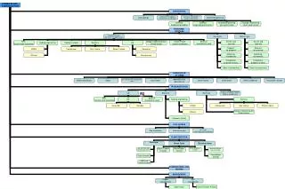
WBS 1.1.1.5.3 Production Schedule M. Garcia-Sciveres - ATLAS Pixel Review - Module Assembly
Development Areas • FE Wafers: Probe bumped,Thin 8”, Mark die, Stress test (wafer burn-in), Dummy wafers. • Electrical Probing: Flex hybrid, Bare module. • Flex Hybrid:Fab. Sources,Wirebonding. • General: Assembly line issues (Q.C., monitoring, etc.), Use dummy modules to address mechanical issues. M. Garcia-Sciveres - ATLAS Pixel Review - Module Assembly