Download
1 / 35
350 likes | 367 Views
Alexander Sudnitson Tallinn University of Technology. IAY 06 0 0 Digital Systems Design. Hazards in Combinational Circuits Timing and Post-Synthesis Verifications. Typical FPGA design flow. Synthesizer.

E N D
Alexander Sudnitson Tallinn University of Technology IAY 0600Digital Systems Design Hazards in Combinational Circuits Timing and Post-Synthesis Verifications
Synthesizer • The objective of a synthesizer is to synthesize logic that behaves identically to the simulated behavior of the design description. A synthesizer translates a design description into a functionally equivalent gate-level logic implementation. • A synthesizer requires two inputs: the design description file and the specification of the target PLD • The synthesizer produces two outputfiles: • A VHDL netlist – a design file that describes, in VHDL structural style, the connectivity of the optimized logic implemented using the target PLD’s primitives. The VHDL netlist is used as UUT model in a post-synthesis simulation. • A technology dependent gate-level netlist. • A netlist is a textual representation of the interconnections.
Synthesizer Typically, a synthesizer performs three steps during synthesis: • Language synthesis: the design description is transformed into a representation based on Boolean equations. • Optimization: algorithms apply the rules of Boolean algebra to optimize the logic for area and /or speed. This optimizations are independent of the technology of the target PLD and produce a technology-independent netlist. • Technology mapping: the logic is mapped to the target PLD. This step corresponds to transforming the technology independent netlist to a technology dependent netlist.
Technology dependent view of half-adder 22V10 SPLD was selected as the target PLD for half-adder design.
Post-synthesis (gate-level) simulation Simulation of the VHDL netlist is called post-synthesis simulation, since it simulates the structural interconnection of the gates and flip-flops synthesized for a design. The results from this simulation are compared with the results from the functional simulation of design description. These results should be the same. If a timing simulation is to be performed, post-synthesis simulation may be skipped.
Place-and-route phase of design flow • A place-and-route (or fitter) tool is software used to automatically map or fit synthesized logic to a target PLD’s architecture. • The place operation selects and configures specific logic primitives in the PLD’s architecture for each logic primitive in the technology dependent netlist. • The route operation determines the path for each connection between a logic primitive and a pin of the PLD. • The place-and-route tool is usually obtained from PLD vendor. • A place-and-route tool uses as its inputs a technology dependent gate-level EDIF netlist and constraint information such as pin assignments for port signals and timing constraints.
Place-and-route phase of design flow • A technology dependent netlist describesthe connectivity of the optimized logic using the target PLD’s logic primitives. These primitives are the logic elements available in the target PLD’s architecture. • The technology dependent netlist is in a format readable by the PLD vendor’s place-and-route tool. Typically, the EDIF netlist format is used. • EDIF ( Electronic Data Interchange Format ) is a format issued by the Electronic Industries Association, as EIE-548. Its purpose is to provide a standard format for transferring design information between EDA tools.
Place-and-route tool outputs • A chip report – which port signals are assigned to which PLD pins and how much of the PLD’s logic capacity is used. • A configuration file (programming file) – contains the interconnection and configuration data necessary to program the PLD. This file specifies exactly which programmable interconnects in the target PLD are to be programmed as connections and which are not. • A VHDL timing model – is a file containing a structural-stile VHDL program that describes the logic and timing of the synthesized logic mapped to the target PLD. This model includes information detailingthe propagation delays of signals through the PLD.
Hazard and glitch A hazard is an output glitch caused by the gate-level structureof acircuit and the propagation delays of its individual gates. A static hazard occurs when a change in the input values to a combinational circuit causes an output to briefly change value when functionally it should have remained the same. This brief change (glitch)is caused by differences in propagation delays through different signal paths in the circuit. A dynamic hazard occurs when a change in the input values to a combinational circuit causes an output to briefly change value multiple times when it should have changed value only once.
Using assertion to verify timing We must consider the possibility of hazards affecting the verification. Look the next slide: In the process, the time between each application of stimulus is given by the constant period. The maximum allowed propagation delay, taken from the systems specification, is given by the constant tpd_spec. After anew stimulus is applied, the process suspends for tpd_spec. When the process resumes, it uses an assertion statement to verify the UUT’s output values. The process then suspends for a time equal to period – tpd_spec.
A description of trivial timing model tb : process constant tpd_spec : time := 11 ns ; constant period: time := 20 ns ; constant n : integer := 2 ; begin --Apply every posiible input combination for i in 0 to 2**n - 1 loop (a_tb, b_tb) <= to_unsigned (i, n) ; -- Verify output values at specified time wait for tpd_spec ; assert ((sum_tb = (a_tb xor b_tb)) and (carry_out_tb = (a_tb and b_tb))) report "test failed for a_tb = " & std_logic ' image (a_tb) & and b_tb = " & std_logic ' image (a_tb) severity error ;
Process to verify logic and timing of model -- Verify that outputs do not subsequently change wait for period - tpd_spec ; assert sum_tb ' quiet (period - tpd_spec) and (carry_out_tb ' quiet (period - tpd_spec) report "propagation delay specification exceded" severity error ; endloop ; wait ; endprocess ; end ;
Timing waveforms When the process (previous slide) again resumes, it verifies that the outputs have not changed since they were last verified. This is accomplished using the signal attribute quite.
Signal-related attributes VHDLcontains anumber ofpredefinedattributeswhich arerelated tosignals : • attributeswhich definesignalsthemselves • attributeswhich arefunctions toprovideinformationabout signals. These attributes are signals themselves
Generics • The VHDL timing model uses a set of timing parameters to specify the propagation delays of the PLD’s primitive elements. • The timing parameter values are usually passed to the model using constants called generics. • Actual generic values are either defined directly in the timing model or specified in a separate file that is generated by the place-and-route tool. • If a separate file is used it usually specifies the generic timing values in a format called standard delay format (SDF). • A PLD’s timing is a function of both the propagation delays of its primitive elements and the specific delay paths that result when the synthesized logic is routed for the target PLD.
Entity declaration that includes generic Generics are similar to constants, except their default values can be overridden from outside of the design entity in which they are declared. Default values can be overridden from outside of the design entity in either: • The component instantiation statement that instantiates the design entity • A configuration declaration.
Trivial timing model for half-adder library ieee; use ieee.std_logic_1164. all; entity half_adder is generic (tpd : time := 10 ns); port (a, b : in std_logic; sum, carry_out : out std_logic); end half_adder; architecturedata_flowof half_adder is begin sum <= a xor bafter tpd ; carry_out <= a and bafter tpd ; enddata_flow;
Remarks Look previous slide: For simplicity, this model uses concurrent signal assignment statements rather than component instantiation statements. This mode has a single generic named tpd. It is used to specify the input to output delay. The advantage of using generics is that we can use the same timing model for different speed grades of the same PLD by simply using the appropriate generic values.
Circuit’s behavior The steady-state behavior of a circuit is the value of the output after the inputs have been stable for a long time. The transient behavior of a circuit is the value of the output while (or soon after) the inputs change. The glitch is a (often undesirable) short pulse produced in the output during a transient phase. If a circuit has the possibility of producing a glitch, the circuit has a hazard.
Static-1 Hazard A static-1 hazard is a set of two input combinations Xa and Xb such that: (i) Xa and Xb differ in only one input variable; (ii) both Xa and Xb produce a 1 output; but it is possible for a momentary 0 to appear in the output when the input transits from Xa to Xb or fromXb to Xa i.e., a static-1 hazard is a possibility of a 0 glitch when we expect a steady 1 output.
Static-0 Hazard A static-0 hazard is a set of two input combinations Xa and Xb such that: (i) Xa and Xb differ in only one input variable; (ii) both Xa and Xb produce a 0 output; but it is possible for a momentary 1 to appear in the output when the input transits from Xa to Xb or from Xb to Xa i.e., a static-0 is a possibility of a 1 glitch when we expect a steady 0 output.
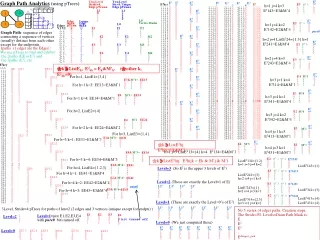
1 1 1 Z Z’ YZ XZ’ F Example Does this circuit have a hazard? If so, of what kind? X XZ’ 0 1 Z’ 0 Z F 0 1 1 0 1 YZ 1 0 The hazard occurs in the transition from X,Y,Z = 111 to X,Y,Z = 110 Y
X 1 1 1 1 1 Z 1 Y Static Hazards in Karnaugh Maps X Z F Y F = X•Z’ + Y•Z How can we identify a static-1 hazard in this Karnaugh map? Two adjacent 1’s that are not in the same term cause a static-1 hazard.
X 1 1 We can add one extra term to F. 1 1 Z F = X•Z’ + Y•Z + X•Y X•Y Y Consensus Term Hazard free design X Z F Y F = X•Z’ + Y•Z How can we eliminate the hazard?
X 1 1 We can add one extra term to F. 1 1 Z X•Y F = X•Z’ + Y•Z + X•Y Y Consensus Term Hazard free designin Karnaugh Maps X Z F Y F = X•Z’ + Y•Z X How can we eliminate the hazard?
W 1 1 1 1 1 1 1 1 1 1 1 1 1 1 1 1 1 1 1 1 X 1 1 Z Z F = W’•Z + X•Z’ + X’•W F = W’•Z + X•Z’ + X’•W 1 1 Y Y Hazard free design:another example To avoid hazards: every par of adjacent 1s should be covered by a 1-term W 1 1 1 1 1 1 1 1 1 1 1 1 X 1. Write minimal form for F 2. Identify static-1 hazards 3. Eliminate static-1 hazards
1 1 Z Z F = W’•Z + X•Z’ + X’•W 1 1 Y Y Hazard free design:another example W W 1 1 1 1 1 1 1 1 1 1 1 1 1 1 1 1 1 1 1 1 1 1 1 1 X X F = W’•Z + X•Z’ + X’•W + X•W’ 1. Write minimal form for F 2. Identify static-1 hazards 3. Eliminate static-1 hazards
1 1 1 1 Z Z F = W’•Z + X•Z’ + X’•W Y Y Hazard free design W W 1 1 1 1 1 1 1 1 1 1 1 1 1 1 1 1 1 1 1 1 1 1 1 1 X X F = W’•Z + X•Z’ + X’•W + X•W’ + W•Z’ 1. Write minimal form for F 2. Identify static-1 hazards 3. Eliminate static-1 hazards
1 1 1 1 Z Z F = W’•Z + X•Z’ + X’•W Y Y Hazard free design W W 1 1 1 1 1 1 1 1 1 1 1 1 1 1 1 1 1 1 1 1 1 1 1 1 X X F = W’•Z + X•Z’ + X’•W + X•W’ + W•Z’ + X’•Z 1. Write minimal form for F 2. Identify static-1 hazards 3. Eliminate static-1 hazards
Dynamic hazards do not occur in properly designed two level AND-OR or OR-AND circuits. PS: A two level AND-OR or OR-AND circuit is properly design if a variable and its complement are never input to the same first level gate. Dynamic hazards A dynamic hazard is the possibility of an output changing more than once as the result of a single transition. Dynamic hazards exist when there are multiple paths with different delays from the changing input to the changing output.
slow 1 1 slower Dynamic hazard example 0 W 0 0 X 0 0 Y 1 1 1 1 1 1 Z
slow 1 0 1 0 slower Dynamic hazard example 0 1 W 0 1 0 X 0 1 0 0 Y 0 1 0 1 1 1 0 0 1 1 1 Z A dynamic hazard occurs when oscilation may occur when a single transition is expected.