Download
1 / 35
370 likes | 550 Views
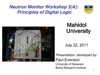
Neutron Monitor Workshop 2(A): Principles of Digital Logic. Mahidol University July 22, 2011 Presentation developed by: Paul Evenson University of Delaware Bartol Research Institute. Workshop Series Idea. Introduce students to technical aspects of neutron monitor operation

E N D
Neutron Monitor Workshop 2(A): Principles of Digital Logic Mahidol University July 22, 2011 Presentation developed by: Paul Evenson University of Delaware Bartol Research Institute
Workshop Series Idea • Introduce students to technical aspects of neutron monitor operation • Rotating workshop series that will repeat every two years at a two per year rate • Independent enough so students can join at any point • Accommodate wide skill range with an emphasis on “hands on” experience and individual discussion
Workshop Series Plan • Detector operation • Detector Physics and Analog Electronics • Art and Science of Soldering • Digital Circuits • Principles of Digital Logic • Neutron Monitor Digital Electronics • Microcontrollers (including data transfer methods within the electronics system) • Real time data acquisition • Principles of Telemetry and Data Acquisition • Data Conversion and Manipulation with Visual Basic
Plan For Today • Lecture with Demonstrations • Describe Hardware Problems and Design Problems • Individual work on design problems • One prototype system here; two people/teams can work at once.
Digital Circuits • Ultimately composed of the same type of electronic components as analog electronics • Digital signals are expressed as analog levels • Typically there are only two logic levels • Called “0” and “1”; “Low” and “High” • Low is usually near ground • High is usually near supply voltage (often +5 volts) • (Bad practice to use supply itself for “High”) • One could define a range of discrete levels but typically this is not done
Simplest Logic Elements • Buffer: Really doesn’t do anything except isolate the input signal and condition the output • Inverter: The circle on an input or output indicates inversion
AND and NAND • Note that you can make any logic function out of NAND gates
OR and NOR • You can also make any logic function out of NOR gates • OR, NOR, AND, NAND all have natural multi-input extensions
XOR (Exclusive OR) • This is the “even parity” operation • Multi input operation is not well defined • One and only one? • Odd number? • All but one?
Simple Implementations • Note that these work, but they are poorly buffered on inputs and outputs, and cannot be combined easily into more complex circuits
Key DC Design Parameters • These tell you: • Voltage ranges for valid 1 and 0 on input • Guaranteed output voltages as a function of load • How much load the gate input puts on the output of anything it is connected to
Key AC Characteristics • Since this is ultimately an analog device it is essential to consider propagation delays in any array of gates • The delays are compounded • Parallel tracks in the logic equation give rise to races and glitches if you are not careful • Often a clock function is used to allow a “settling time” and then to record (or “register” the output before proceeding to the next step in the device operation
Digital Signal Requirements • Signals must never remain in “never-never land”. At a minimum this increases power draw and may damage the chip • Transitions must be monotonic and “fast” • Slow or sloppy transitions must be conditioned by triggers or discriminators • If the signals are only slow, most logic families include devices with Schmidt trigger inputs • Mechanical contacts must be de-bounced
Simple Memory – Set/Reset Flip-Flop • Pushing a button sets (A) or resets (B) the device • This state remains until the other button is pushed • “Set” and “Reset” describe the device state – one output is always the complement of each other
The Clocked “D” Flip-Flop • On the leading edge of the clock, the state of D is remembered in the outputs • The state is remembered before the outputs change • Therefore the outputs may be fed back into the logic that determines the input without ambiguity
One-Shots • A “one-shot” produces a pulse in response to a “leading edge” on the input • The opposite transition produces no response • If a precise (or very long) pulse duration is needed, use a device where this is controlled by analog components
Simple One-Shot for Edge Triggering • Produces a short pulse on positive edge • No reaction to the following negative edge • Duration is a function of temperature, supply voltage, and device variation • If implemented with devices in the same logic family the pulse is usually long enough with one inverter • More buffers or inverters will lengthen it (to a point) Add buffers or inverters (in pairs) here to lengthen the pulse
Ripple Counter from D Flip-Flops • When clocked, each D changes state because Qbar is fed back into D • When and only when Qbar rises the next flipflop is clocked • Each thus operates at half the rate of the previous stage forming a counter • Because of the ripple, not all stages change state at the same time so the count is actually only well defined after a settling time • Synchronous counters also exist, where all outputs change simultaneously • Even there, the finite time of the transition can cause glitches
Shift Registers • The ripple counter becomes a “shift register” if Q of one stage is connected to D of the following, and all the clocks are connected together http://en.wikipedia.org/wiki/Shift_register
Johnson Counter – Multiphase Clock • A shift register loaded with a single “1” becomes what is known as a Johnson Counter • The “1” moves from stage to stage, and is often the simplest way to sequence logic and allow for setup time • Fed back on itself this becomes a “multiphase clock” • Typically only the “even” phases are used to sequence logic, ensuring that there is no overlap and good settling time Modified from http://en.wikipedia.org/wiki/Shift_register
Problem 1: Implement the following using only NAND gates • Buffer • Inverter • AND • OR • XOR (Exclusive Or)
Problem 2: Explain How This Circuit “Debounces” the Contacts
Problem 3: How a D Flipflop Works • Figure out how gate delays implement the edge triggered feature of the D flipflop • Using the chips on the prototype board build this circuit and use it to add one more stage to the counter Note that this is just our old friend, the set-reset flipflop
Problem 5: Design an 8 Bit “Accumulator” to Add 4 Bit Numbers • An accumulator is an array of memory cells to which successive numbers can be added • Use four of the switches for input • Use one of the push buttons as a clock • Display the results in the lights
Problem 6: Design a Circuit to Multiply Two 4 Bit Numbers • Multiplying two, four bit numbers yields an eight bit product • This actually could be implemented with a lot of gates, since there is an 8 bit 8 bit truth table that uniquely specifies the answer, but here you should do it with clocked logic • Use two groups of four switches for the inputs • Display the product in the lights • Use a push button to initiate the clock sequence
Problem 3: How a D Flipflop Works 1 0 1* 1 1 Q0 1* Q0 0 1* 1 • Figure out how gate delays implement the edge triggered feature of the D flipflop • Using the chips on the prototype board build this circuit and use it to add one more stage to the counter 0 1 Note that this is just our old friend, the set-reset flipflop 1* 0
Problem 3: How a D Flipflop Works 1 0 1* 1 1 Q0 1* Q0 0 1* 1 • Figure out how gate delays implement the edge triggered feature of the D flipflop • Using the chips on the prototype board build this circuit and use it to add one more stage to the counter 0 1 Note that this is just our old friend, the set-reset flipflop 1* 0
Problem 3: How a D Flipflop Works 1 0 1 1 0 1 0 1 1 0 0->1 0 1 • Figure out how gate delays implement the edge triggered feature of the D flipflop • Using the chips on the prototype board build this circuit and use it to add one more stage to the counter 1 0 0 1 Note that this is just our old friend, the set-reset flipflop
Problem 3: How a D Flipflop Works 1 0 1 1 0 1 0 1 1 0 1 0 1 • Figure out how gate delays implement the edge triggered feature of the D flipflop • Using the chips on the prototype board build this circuit and use it to add one more stage to the counter 0->1* 1 0->1 1->0 Note that this is just our old friend, the set-reset flipflop
Problem 3: How a D Flipflop Works 1 0 1 1 0 1 0 1 1 0 1->0 0->1* 1 • Figure out how gate delays implement the edge triggered feature of the D flipflop • Using the chips on the prototype board build this circuit and use it to add one more stage to the counter 1 0 0 1 Note that this is just our old friend, the set-reset flipflop
Problem 3: How a D Flipflop Works 0 1 1 x 1 0 x 1 • Figure out how gate delays implement the edge triggered feature of the D flipflop • Using the chips on the prototype board build this circuit and use it to add one more stage to the counter 0 1 Note that this is just our old friend, the set-reset flipflop 1* 0
Problem 3: How a D Flipflop Works 1 ? 0 1 0 1 x ? ? • Figure out how gate delays implement the edge triggered feature of the D flipflop • Using the chips on the prototype board build this circuit and use it to add one more stage to the counter 0 1 Note that this is just our old friend, the set-reset flipflop