Download
1 / 35
350 likes | 502 Views
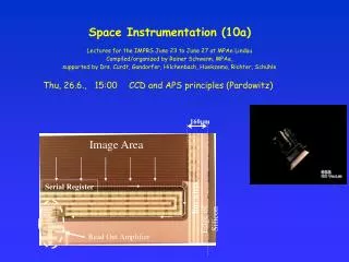
160 m m. Image Area. Serial Register. Bus wires. Edge of Silicon. Read Out Amplifier. Image Detectors: CCD and APS. Introduction CCD history CCD structure Charge generation and collection Charge transfer & readout APS principles Performance parameters of CCD‘s. I. Pardowitz.

E N D
160mm Image Area Serial Register Bus wires Edge of Silicon Read Out Amplifier
Image Detectors:CCD and APS • Introduction • CCD history • CCD structure • Charge generation and collection • Charge transfer & readout • APS principles • Performance parameters of CCD‘s I. Pardowitz IMPRS – 26.6.2003
Images and reality GALILEI: Ich habe das unvorstellbare Glück gehabt, ein neues Instrument in die Hand zu bekommen, mit dem man ein Zipfelchen des Universums etwas, nicht viel, näher besehen kann. Benutzen Sie es. ... GALILEI: Mensch, reg dich auf! Was du siehst, hat noch keiner gesehen. (B. Brecht „Leben des Galilei“)
ħω From photon to knowledge ...010011010101... interpretation measurement photoeffect e-
Evolution of space CCD‘s OSIRIS Yohkoh Galileo & HST Pathfinder HMC First Fairchild CCD
Structure of a CCD (1) Channel stops to define the columns of the image Plan View Transparent horizontal electrodes to define the pixels vertically. Also used to transfer the charge during readout One pixel Electrode Insulating oxide n-type silicon p-type silicon Cross section Every third electrode is connected together. Bus wires running down the edge of the chip make the connection. The channel stops are formed from high concentrations of Boron in the silicon.
Structure of a CCD (2) Below the image area (the area containing the horizontal electrodes) is the ‘Serial register’ . This also consists of a group of small surface electrodes. There are three electrodes for every column of the image area Image Area On-chip amplifier at end of the serial register Serial Register Cross section of serial register Once again every third electrode is in the serial register connected together.
160mm Image Area Serial Register Bus wires Edge of Silicon Read Out Amplifier Structure of a CCD (3) Photomicrograph of a corner of an EEV CCD. The serial register is bent double to move the output amplifier away from the edge of the chip. This useful if the CCD is to be used as part of a mosaic.The arrows indicate how charge is transferred through the device.
Electric Field in a CCD (1) depletion width: Electric potential Electric potential W Potential along this line shown in graph above. p p
Electric Field in a CCD (2) The n-type layer contains an excess of electrons that diffuse into the p-layer. The p-layer contains an excess of holes that diffuse into the n-layer. This structure is identical to that of a diode junction. The diffusion creates a charge imbalance and induces an internal electric field. The electric potential reaches a maximum just inside the n-layer, and it is here that any photo-generated electrons will collect. All science CCDs have this junction structure, known as a ‘Buried Channel’. It has the advantage of keeping the photo-electrons confined away from the surface of the CCD where they could become trapped. It also reduces the amount of thermally generated noise (dark current). Electric potential Electric potential Potential along this line shown in graph above. n p Cross section through the thickness of the CCD
Electric Field in a CCD (3) During integration of the image, one of the electrodes in each pixel is held at a positive potential. This further increases the potential in the silicon below that electrode and it is here that the photoelectrons are accumulated. The neighboring electrodes, with their lower potentials, act as potential barriers that define the vertical boundaries of the pixel. The horizontal boundaries are defined by the channel stops. Electric potential Region of maximum potential n p
p-type silicon n-type silicon Charge Collection in a CCD (1) Photons entering the CCD create electron-hole pairs. The electrons are then attracted towards the most positive potential in the device where they create ‘charge packets’. Each packet corresponds to one pixel diffusion length: pixel boundary pixel boundary incoming photons Electrode Structure Charge packet SiO2 Insulating layer
Pixel size & Dynamic Range Charge Collection in a CCD (2) Spectral sensitivity a.) Absorption depth in Si tox≈0,2-1µm b.) Charge capacity per unit area incoming photons C≈1012 e-/cm2 typ. pixel size= (10µm)2 charge capacity = 50-200 103 e-/pixel Blooming
1 2 3 Charge Transfer in a CCD (1) In the following few slides, the implementation of the ‘conveyor belts’ as actual electronic structures is explained. The charge is moved along these conveyor belts by modulating the voltages on the electrodes positioned on the surface of the CCD. In the following illustrations, electrodes colour coded red are held at a positive potential, those coloured grey are held at a negative potential.
1 2 1 2 3 3 Charge Transfer in a CCD (2) +5V 0V -5V +5V 0V -5V +5V 0V -5V Time-slice shown in diagram
1 2 1 2 3 3 Charge Transfer in a CCD (3) +5V 0V -5V +5V 0V -5V +5V 0V -5V
1 2 1 2 3 3 Charge Transfer in a CCD (4) +5V 0V -5V +5V 0V -5V +5V 0V -5V
1 2 1 2 3 3 Charge Transfer in a CCD (5) +5V 0V -5V +5V 0V -5V +5V 0V -5V
1 2 1 2 3 3 Charge Transfer in a CCD (6) +5V 0V -5V +5V 0V -5V +5V 0V -5V
1 2 1 2 3 3 Charge Transfer in a CCD (7) +5V 0V -5V Charge packet from subsequent pixel enters from left as first pixel exits to the right. +5V 0V -5V +5V 0V -5V Charge Transfer Efficiency Radiation
1 2 1 2 3 3 Charge Transfer in a CCD (8) +5V 0V -5V +5V 0V -5V +5V 0V -5V
R R Readout Circuit of a CCD Photomicrograph of the on-chip amplifier of a Tektronix CCD and its circuit diagram. Output Drain (OD) 20mm Gate of Output Transistor SW RD OD Output Source (OS) Output Node Reset Transistor Reset Drain (RD) Summing Well Output Node Output Transistor Serial Register Electrodes OS Summing Well (SW) Substrate Last few electrodes in Serial Register
R R On-Chip Amplifier (1) The on-chip amplifier measures each charge packet as it pops out the end of the serial register. +5V 0V -5V RD and OD are held at constant voltages SW SW RD OD +10V 0V Reset Transistor Vout Summing Well Output Node Output Transistor --end of serial register (The graphs above show the signal waveforms) OS The measurement process begins with a reset of the ‘reset node’. This removes the charge remaining from the previous pixel. The reset node is in fact a tiny capacitance (< 0.1pF) Vout
R R On-Chip Amplifier (2) The charge is then transferred onto the Summing Well. Vout is now at the ‘Reference level’ +5V 0V -5V SW SW RD OD +10V 0V Reset Transistor Vout Summing Well Output Node Output Transistor --end of serial register OS There is now a wait of up to a few tens of microseconds while external circuitry measures this ‘reference’ level. Vout
R R On-Chip Amplifier (3) The charge is then transferred onto the output node. Vout now steps down to the ‘Signal level’ +5V 0V -5V SW SW RD OD +10V 0V Reset Transistor Vout Summing Well Output Node Output Transistor --end of serial register OS This action is known as the ‘charge dump’ Vout Noise
R R On-Chip Amplifier (4) Vout is now sampled by external circuitry for up to a few tens of microseconds. +5V 0V -5V SW SW RD OD +10V 0V Reset Transistor Vout Summing Well Output Node Output Transistor --end of serial register OS The sample level - reference level will be proportional to the size of the input charge packet. Vout
Active Pixel Sensors (1) with photodiode with photogate Vdd Vdd Vdd Vdd Reset Reset Transistor Reset Reset Transistor TX PG Column Bus Column Bus Select Output Transistor Select Output Transistor
APS readout CMOS = 2T APS (3T) APS
Performance Parameters(1) • Spectral range • QE = quantum efficiency • Noise • Dynamic range • CCE = Charge Collection Efficiency • Dark current • CTE = Charge Transfer Efficiency
Performance Parameters (2) • Number of pixels • Framerate • Radiation hardness • Power requirements • Chip count • Technology / Market / Price
Signal-to-Noise Quelle: James Janesick. 2002
Other detectors • PtSi (3-5 um) • HgCdTe (3-5 or 8-10 um) • CdZnTe • QWIP (8-10 um) • AlGaN (300 nm)