Lecture 9.1
300 likes | 455 Views
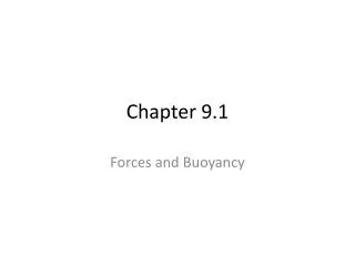
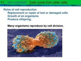
Lecture 9.1. Building a FET. Integrated Circuits. CPU or Memory First Layer Transistors Capacitors Diode Resistors Multi-layer Wiring Interconnects Bonding Pads Dielectric Capacitors Heterostructures. MOSFET in Memory Chip. Source Gate Drain. Field Effect Transistor (FET).

Lecture 9.1
E N D
Presentation Transcript
Lecture 9.1 Building a FET
Integrated Circuits • CPU or Memory • First Layer • Transistors • Capacitors • Diode • Resistors • Multi-layer • Wiring • Interconnects • Bonding Pads • Dielectric • Capacitors • Heterostructures
MOSFET in Memory Chip Source Gate Drain
Make Mask for Doping • Clean wafer surface • Oxidize Si Surface • How Thick is needed for Doping Mask? • Spin on photoresist • Image photoresist • Develop photoresist • Dissolve un-crosslinked photoresist • Etch exposed SiO2 down to the Si of the wafer • Doping • Remove Implantation Mask
Silicon Oxidation • Reactor • Furnace at T=850C • Pure Oxygen • Si + O2 SiO2 • Kinetics • BL-Mass Transfer • J=Kg(CA-0) • SS-Diffusion • J=DO-SiO2 (dC/dx) • Heat Transfer • BL, q=h(T1-T) • Solid, q=kSiO2(dT/dx) • J=q/Hrxn Grxn<0, Spontaneous
Kinetics • Thickness • Linear Rate • Reaction Control • First Order • BL-MT Control • BL-HT Control • Parabolic Rate • Product diffusion Control • Product heat transfer Control • J =(dx/dt) SiO2/MW SiO2
Thickness Experiments • Parabolic Rate • Derive it! • dx2/dt=2K • K=Ko exp(-Ea/RgT) • x=o @ t=0 • x= at t= • Very common!! • Slow Solid State Diffusion • Slow Heat Conduction
Mask Thickness • To effectively prevent ions penetrating in thick zone • Relatively thick Oxide Protection layer • Patterned • Thinning (etching) of Oxide Protection layer over implantation zone • Remove oxide layer with impurities inside
Mask Thickness • Transmission through mask • T=1/2 erfc[(x-xave)/2 x] • To stop 99.99% of implanted materials, T=10-4 • Solve for x, the thickness to stop 99.99% of ions.
Implantation • Create Ions in Vacuum • Accelerate in Electric Field • Impinge onto Silicon Surface • Knock out Si ion(s) • Charge Balance • Travel deep into Silicon
Implantation • Effect of Ion Mass
Implant Depth Depth Increases with Energy
Implantation Straggle Increases with Energy
Implantation Concentration Profile • Probability Based • N(x)=Nmax exp[(x-xave)2/2x2] • Nmax=(Ndose/[(2) x])~(0.4 Ndose/ x) • Ndose=Qdose/e • Qdose= current applied/cm2 • σx = projected straggle
Remove Implantation Mask • Chemical Mechanical Polishing • Remove all Oxide from wafer surface • Dry Etching
Drive Dopant Impurities into Wafer • Heat Treating • Laser Annealing • Diffusion • Heat and Hold for period of time • Solid State Diffusion • dC/dt=D d2C/dx2 • C=Co at x=0 • C=0 at x=
Diffusion of Implanted Dopants • Diffusion Furnace or Laser • Heat Treatment • Solid State Diffusion • dCA/dt = CT d/dz(DAB dXA /dz) • C=Co(z) = CT XA(z) at z=0 • C=0 at z= • DAB =(D*A XB + D*B XA) (d ln [aA]/d ln [XA]) • Interdiffusion or mutual diffusion coefficient
Gate Oxide • Capacitor connecting Gate to center of npn or pnp heterojunction • Capacitance • Area • Thickness • Dielectric constant of oxide
Gate Oxide Capacitance C=oA/d =C/Co =1+e e = electric susceptibility
Thickness Experiments • Parabolic Rate • Derive it! • dx2/dt=2K • K=Ko exp(-Ea/RgT) • x=o @ t=0 • x= at t= • Very common!! • Slow Solid State Diffusion • Slow Heat Conduction
Metalization • Transistor Contacts • Base • Emitter • Gate • Planarize/Polish layer to get Flat Surface for next lithography Step • Metal Deposition