Download
1 / 1
10 likes | 130 Views
Silicon Drift Detectors (SDDs), introduced by Gatti and Rehak in 1984, have revolutionized X-ray spectroscopy, being integral in various scientific fields and industrial applications. Their key advantages include operation close to room temperature, high spectral resolution, and excellent count rate capabilities. This is attributed to low readout node capacitance and specific fabrication processes. Recent advancements include analyzing historical manuscripts and Martian soil samples, showcasing SDDs' versatility and importance in both research and practical applications.

E N D
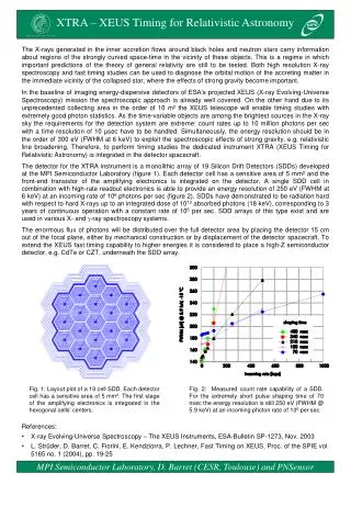
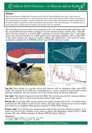
Silicon Drift Detectors - in Heaven and on Earth Abstract Silicon Drift Detectors (SDDs) have been proposed in 1984 by Gatti and Rehak. Since then a large variety of detectors for room temperature X-ray spectroscopy have been used in many different fields of science. In addition to their implementation in complex scientific instruments, they are used today in thousands of industrial applications in the field of quality asssurance & control and material characterization. Their main advantage is its operation close to room temperature, the high spectral resolution and the high count rate capability. The basic physical reason of the above properties is the very small readout node capacitance and the special fabrication procedures, leading to very low thermal leakage currents. Fig. 1 (top left) shows the basic design of a circular SDD, including the on-chip electronics, Fig. 2 (top right) depicts the electrical potential of a SDD under typical operating conditions. The on-chip JFET in the center prepares the signals for further shaping and amplification. The achieved energy resolution is around 130 eV (FWHM) at 6 keV and 10.000 counts per second. Top left: Basic design of a circular silicon drift detector with an integrated single sided JFET inside. The backside of the SDD has a homogeneous p+ contact, negatively biased under normal operating conditions. The most positive area is the readout anode for electron collection. Top right: The electrical potential inside the SDD. All electrons generated by ionizing radiation have to end after 100 ns at most at the positively biased ande contact. Bottom left: A scanning SDD system analyzes the original manuscript of J.W. von Goethes Faust I and Faust II. The analysis of the ink has shown, that some parts of Faust I have been rewritten after Faust II was completed (Measurement made by O. Hahn, BAM, Berlin) Bottom right: X-ray fluorescence measurements with martian soil from different locations. A Cu source was used for the exitation of the atoms on Spirit and Opportunity aboard NASA´s MER mission. (PI of the APXS instrument: R. Rieder, MPI für Chemie, Mainz). • References: • E. Gatti, P. Rehak, NIMA, 225, page 608 – 621, 1984 • L. Strüder, SPIE, Vol. 4141, page 29 – 48, 2000 MPI Semiconductor Laboratory and PNSensor