Download
1 / 17
170 likes | 394 Views
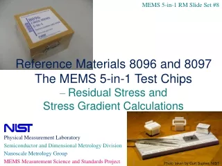
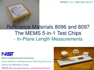
MEMS 5-in-1 RM Slide Set #10. Reference Materials 8096 and 8097 The MEMS 5-in-1 Test Chips – Thickness Measurements (for RM 8097). Physical Measurement Laboratory Semiconductor and Dimensional Metrology Division Nanoscale Metrology Group MEMS Measurement Science and Standards Project.

E N D
MEMS 5-in-1 RM Slide Set #10 Reference Materials 8096 and 8097 The MEMS 5-in-1 Test Chips – Thickness Measurements (for RM 8097) Physical Measurement Laboratory Semiconductor and Dimensional Metrology Division Nanoscale Metrology Group MEMS Measurement Science and Standards Project Photo taken by Curt Suplee, NIST
Outline for Thickness Measurements (for RM 8097)
1. References to Consult • Overview 1. J. Cassard, J. Geist, and J. Kramar, “Reference Materials 8096 and 8097 – The Microelectromechanical Systems 5-in-1 Reference Materials: Homogeneous and Stable,” More-Than-Moore Issue of ECS Transactions, Vol. 61, May 2014. 2. J. Cassard, J. Geist, C. McGray, R. A. Allen, M. Afridi, B. Nablo, M. Gaitan, and D. G. Seiler, “The MEMS 5-in-1 Test Chips (Reference Materials 8096 and 8097),” Frontiers of Characterization and Metrology for Nanoelectronics: 2013, NIST, Gaithersburg, MD, March 25-28, 2013, pp. 179-182. 3. J. Cassard, J. Geist, M. Gaitan, and D. G. Seiler, “The MEMS 5-in-1 Reference Materials (RM 8096 and 8097),” Proceedings of the 2012 International Conference on Microelectronic Test Structures, ICMTS 2012, San Diego, CA, pp. 211-216, March 21, 2012. • User’s guide (Section 8, pp. 137-156) 4. J.M. Cassard, J. Geist, T.V. Vorburger, D.T. Read, M. Gaitan, and D.G. Seiler, “Standard Reference Materials: User’s Guide for RM 8096 and 8097: The MEMS 5-in-1, 2013 Edition,” NIST SP 260-177, February 2013 (http://dx.doi.org/10.6028/NIST.SP.260-177). • Standard 5. SEMI MS2-1113, “Test Method for Step Height Measurements of Thin Films,” November 2013. (Visit http://www.semi.org for ordering information.) • Thickness article 6. J.C. Marshall, “New Optomechanical Technique for Measuring Layer Thickness in MEMS Processes,” J. of Microelectromechanical Systems, Vol. 10, No. 1, pp. 153-157, March 2001. • Fabrication 7. The RM 8097 chips were fabricated at MEMSCAP using MUMPs-Plus! (PolyMUMPs with a backside etch). The URL for the MEMSCAP website is http://www.memscap.com.
2a. Thickness (for RM 8097) Overview • Description: The height of one or more thin-film layers • Purpose: Used in the determination of thin film material parameters, such as Young’s modulus • Test structure: Cantilever exhibiting stiction • Instrument: Interferometric microscope, stylus profilometer, or comparable instrument(s) • Method: Calculated from step height measurements of: a) the height of the anchor to the underlying layer (A), b) the height of the stuck portion of the cantilever to the anchor (B), and/or c) the height of the stuck portion of the cantilever to the underlying layer (C) C
2b-2c. P1 or P2 Thickness Equationsand Data Sheet Uncertainty Equations (for RM 8097) where Aheight from the underlying layer to the anchor Bheight from the anchor to the top of the stuck portion of the cantilever Ccalccalculated height from the underlying layer to the top of the stuck portion of the cantilever Hanchor etch depth Jheight from the top of the underlying layer to the bottom of the stuck portion of the cantilever that takes into consideration the roughness of the surfaces, any residue present between the layers and a tilting component
2b-2c. P1 or P2 Thickness Equations and Data Sheet Uncertainty Equations (for RM 8097) • Determine the thickness, α, three different ways: • Choose the value for α(i.e., αi, αii, orαiii) that has the smallest uncertainty unless the value for α has been preselected • The data sheet (DS) expanded uncertainty equation is where k=2 is used to approximate a 95 % level of confidence
2d. ROI Uncertainty Equation UROI expanded uncertainty recorded on the Report of Investigation (ROI) UDS expanded uncertainty as obtained from the data sheet (DS) Ustability stability expanded uncertainty
3. Location of Cantilever on RM 8097(The RM 8097 Chips) • RM 8097 • Fabricated using a polysilicon multi-user surface-micromachining MEMS process with a backside etch • Material properties of the first or second polysilicon layer are reported • Chip dimensions: 1 cm x 1 cm Lot 98 Lot 95
3. Location of Cantilever on RM 8097 Top view of thickness test structure Locate the cantilever in one of these groups given the information on the NIST-supplied data sheet 10
4. Test Structure Description (For RM 8097) Top view of thickness test structure
4. Test Structure DescriptionFor RM 8097 p1 p2 Top view of thickness test structures Top view of cantilevers in in-plane length group p2 Unconventional anchor design Same anchor design as in thickness test structures p1
5. Calibration Procedure • Calibrate instrument in the z-direction • As specified for step height calibrations
6. Measurement Procedure • Measure A (using a stylus profilometer) – optional • Obtain 3 data traces • Level the data with respect to the poly0 layer • From platX • Obtain platXa1, platXb1, and platXc1 • Obtain splatXa1, splatXb1, and splatXc1 • From platY • Obtain platYa1, platYb1, and platYc1 • Obtain splatYa1, splatYb1, and splatYc1 • Measure C (using an optical interferometer) • Use a high magnification objective • Obtain 3 data traces (typically perpendicular to the beam and crossing the pegged portion of the beam) • Level the data with respect to the poly0 layer • From platZ • Obtain platZa2, platZb2, and platZc2 • Obtain splatZa2, splatZb2, and splatZc2 • From platX • Obtain platXa2, platXb2, and platXc2 • Obtain splatXa2, splatXb2, and splatXc2 C
6. Measurement Procedure (continued) • Obtain • From the NIST-supplied data sheet: • repeat(samp)Nrelative step height repeatability standard deviation • H anchor etch depth • H range of the anchor etch depth • Jest estimated value for the dimension J • ucJestestimate for the combined standard uncertainty of Jest • sroughXsmallest of all the values obtained for splatXt1and splatXt2 • sroughY =sroughZ smallest of all the values obtained for splatYt1andsplatZt2 • Typically, choose • Fate of A = 1 to disregard i as a possible thickness • Fate of B = 1 to disregard iias a possible thickness • Fate of C> 0 if > 0, to force the selection of iii (calculated using C and Jest) as the thickness if = 0, to let the software determine the thickness by the smallest uncertainty value C
7. Using the Data Sheet • Find Data Sheet T.3.a • On the MEMS Calculator website (Standard Reference Database 166) accessible via the NIST Data Gateway (http://srdata.nist.gov/gateway/) with the keyword “MEMS Calculator” • Note the symbol next to this data sheet. This symbol denotes items used with the MEMS 5-in-1 RMs. • Using Data Sheet T.3.a • Click “Reset this form” • Supply INPUTS to Tables 1 through 4 • Click “Calculate and Verify” • At the bottom of the data sheet, make sure all the pertinent boxes say “ok.” If a pertinent box says “wait,” address the issue and “recalculate.” • Compare both the inputs and outputs with the NIST-supplied values
8. Using the MEMS 5-in-1To Verify RM 8097 Thickness Measurements • If your criterion for acceptance is: where Dα positive difference between the thickness value of the customer, α(customer), and that appearing on the ROI, α Uα(customer) thickness expanded uncertainty of the customer Uα thickness expanded uncertainty on the ROI, UROI • Then can assume measuring the poly1 (or poly2) thickness according to SEMI MS2 according to your criterion for acceptance if: • Criteria above satisfied and • No pertinent “wait” statements at the bottom of your Data Sheet T.3.a