Download

1 / 14
140 likes | 168 Views
Learn about the design, production, and unique features of PHOBOS silicon sensors, including specifications, milestones, sensor dimensions, assembly details, and test criteria.

E N D
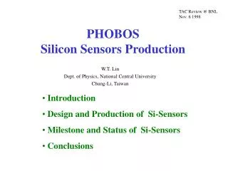
TAC Review @ BNL Nov. 6 1998 PHOBOS Silicon Sensors Production W.T. Lin Dept. of Physics, National Central University Chung-Li, Taiwan • Introduction • Design and Production of Si-Sensors • Milestone and Status of Si-Sensors • Conclusions
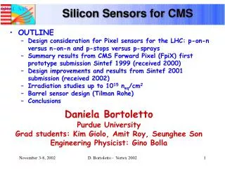
Unique feature of PHOBOS A single detector technology for almost the whole experiment • Silicon detectors (pad and strip): • small pad for high density detection • truly two dimensional readout • well developed technology 438 Silicon sensors with 134,832 channels
Sensors for PHOBOS expt. Type Assembly Spare Total 1-arm Spectrometer 1 8 4 12 2 14 14 28 3 28 14 42 4 21 14 35 5 66 20 86 Multiplicity counter Oct 92 18 110 Ivtx 8 2 10 Ovtx 16 4 20 Ring 48 12 60
Phobos Silicon Sensors The electric characteristic of each component can be measured from test keys Bulk 320+/- 30 mm 1st metal 5000 A 2nd metal 20000 A SOG 12000 A ONO 3200 A VF.D. < 70 V Ileak = 1 - 5 mA Rpoly> 1 MW CSOG= 40 +/- 2 pF/mm2 CONO = 170 +/- 5 pF/mm2
Design of PHOBOS Silicon Sensors AC-coupled Direct bias Double metalization signal lines -V bias bus ONO thin oxide metal 2 vias SOG thick oxide metal 1 320mm 5KW-cm Signal p+ Implant Polysilicon Drain Resistor n+ Implant +V
Dimensions of Sensors Type Dimen. Of Sensor Dimen. Of Pad channels 1 7.16x3.78(cm) 940x940(mm) 1536 2 8.04x4.485 5940x367 500 3 8.04x4.4838 7440x607 512 4 8.04x4.4838 14940x607 256 5 7.98x4.43 18940x607 256 Oct 8.41x3.63 8650x2648 120 Ivtx 6.2104x5.04 11975x413 512 Ovtx 6.2104x5.04 24010x413 256 Ring 11>R>5 45deg varies 64 Pad size from 1 mm2 to 23 mm2 Gap btw pads 60 mm Width of signal traces 15 mm Gap btw traces >35 mm
Mask Design • 6 masks to define 1st : P+(Implant 0.8mm) 2nd: Polysilicon (L:250mm, W:15mm) 3rd: Contact window (L:10mm, W:10mm) 4th: Metal 1(T:0.5mm) 5th: Via (L:15mm, W:15mm) 6th: Metal 2 (T:1.2mm, W:15mm) • 34 Stages to process Normal run : 0.8 - 1 stage/day Hot run : 1.5 - 2 stage/day
CV Scan Type-1 : 1536 channels Time consume: 128-180 min/wafer
Criteria of Accepted Sensor • Rpoly > 1 MW • Ileak < 5 mA @ (1.1)*VFD or • Ileak < 10 mA with a flat IV line shape • Yield of pinhole < 3% • VFD < 70V
Status of Spectrometer 1-arm spectrometer NeedNCU MIT Tested Accepted Rejected Type-1 12 66 27 17 10 Type-2 28 89 10 7 3 Type-3 42 23 64 23 18 5 Type-4 35 39 50 48 45 3 Type-5 86 100114 105 67 38
Milestone of Spectrometer WBS milestone Sensor delivered Jan Feb Mar Apr May Jun Jul Aug Sep Oct Nov Dec Type-1 7 12 24 31 Type-2 7 9 28 63 Type-3 7 5 9 7 41 2337 Type-4 7 43 2539 20 Type-5 4616 50 35 40 25 100
Status of Multiplicity Counter Need NCU UICTested Accepted Rejected Octagon 110 8258 53 23 30 Inner 10 13 13 8 5 Outer 2039 7 7 3 4 Ring 6060 70 58 41 17 Need 1 batch of inner vtx and 4 batches of octagon to fulfill multiplicity detector.
Milestone of Multiplicity Counter WBS milestoneSensor delivered ‘98 Jan Feb Mar Apr May Jun Jul Aug Sep Oct Nov Dec Octagon 12 10 1102 34 82 Inner Vtx 7 10 1 5 Outer Vtx 3 4 2039 Ring 6070 60 Annual shut down for maintenance is during Chinese New Year. ERSO changed a brand new implanter.
Conclusions • Most silicon wafer production has been • completed and sensors now being tested. • Most of production was on time except • for type-5 and octagon.