ECE 4110– Sequential Logic Design
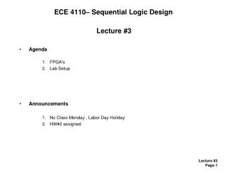
ECE 4110– Sequential Logic Design. Lecture #3 Agenda FPGA's Lab Setup Announcements No Class Monday , Labor Day Holiday HW#2 assigned. Digital Design Flow. Designing Large Circuits - this is the ideal process. Digital Design Flow. Designing Large Circuits - this is reality. FPGA's.

ECE 4110– Sequential Logic Design
E N D
Presentation Transcript
ECE 4110– Sequential Logic Design Lecture #3 • Agenda • FPGA's • Lab Setup • Announcements • No Class Monday , Labor Day Holiday • HW#2 assigned
Digital Design Flow • Designing Large Circuits- this is the ideal process
Digital Design Flow • Designing Large Circuits- this is reality
FPGA's • What is an FPGAField Programmable Gate Array • An FPGA uses Re-configurable Logic Blocks- we set the config bits of this block to set its Boolean logic function- the configuration is a Truth Table (or Look Up Table) of functionality configOut 000 NOT(In1) 001 NOT(In2)010 OR 011 NOR 100 AND 101 NAND 110 XOR111 XNOR In1 Out In2 config
In1 In1 In1 In1 In1 In1 In1 In1 In1 Out Out Out Out Out Out Out Out Out In2 In2 In2 In2 In2 In2 In2 In2 In2 config config config config config config config config config FPGA's • LUTs = Look Up Tables- we can program the LUTs to be whatever type of gate is needed by the design- there are a finite number of LUTs within a given FPGA (also called "resources") • The LUTs are configured into an ARRAY on the silicon- Array of LUT's = Array of Gates = Gate Array
LUT LUT LUT LUT LUT LUT LUT LUT LUT FPGA's • Programmable Interconnect - there are programmable interconnect switches that connect the LUTs X X X X X X X X X X X X X X X X X
LUT LUT LUT LUT LUT LUT LUT LUT LUT FPGA's • Configuration- We start with a Gate Level Schematic of our design (from synthesis)- The FPGA LUTs are configured to implement Gates X X X X X X X X X X X X X X X X X
LUT LUT LUT INV OR LUT INV AND LUT FPGA's • Configuration- The interconnect switches are then programmed to implement the net connections A X X B Out X X X X X C X X X X X X X X X X
LUT LUT LUT INV OR LUT INV AND LUT FPGA's • Configuration- The LUT and Interconnect configuration is volatile (i.e., it goes away when power is removed)- Since the programming is done by the user after fabrication, we call it "Field Programmable"- We now understand where Field Programmable Gate Array A X X B Out X X X X X C X X X X X X X X X X
CLB CLB CLB CLB FPGA's • Adding More Functionality - FPGA manufacturer's quickly learned that Flip-Flops would be useful- They put a DFF next to a 4-Input LUT to form a "Configurable Logic Block" (CLB), • CLB also known as Logic Element (LE) X X X X X
FPGA's • Adding Even More Functionality - To Improve performance, common logic functions were "hard coded" on the silicon - Block RAM - Adders / Multipliers - Global Clock Buffers - even Microprocessors!
FPGA's • What else can we program? - Which Pins to use on the package- What logic levels - CMOS_33, CMOS25 - SSTL, SSTL2, etc…
Lab Setup We will use the Altera UP1 FPGA board (found in the CAD Lab) • PLD Part Numbers • Max7128 = EPM7128SLC84-7 • Flex10k = EPF10K20RC240-4 or EPF10K70RC240-4 • On-board jumper settings • For Max7128 only: Set all 4 jumpers to the UP (TOP) position. • For Flex10k20 only: Set the 4 jumpers to DOWN DOWN UP UP position respectively. • LEDs, Switches, Seven-Segments • VGA, mouse ports • 25.175 MHz oscillator • EEprom to hold FPGA program • 3 expansion ports, each with 42 I/O pins • 7 global pins • (user's guide on website)
Lab Setup • Programming the FPGA- Boundary Scan (JTAG) - a daisy chain protocol that allows programming of chips- FPGA - we can program the FPGA direction - volatile nature means if we remove power, we'll loose program- EEprom - we can download our code into an on-board EEprom - Upon power up, the EEprom will program the FPGA NOTE: We'll mostly program the FPGA directly
Lab Setup Programming the FPGA • Compile the top-level project for the appropriate Max EPM7128SLC84-7 or Flex EPF10K20 or Flex EPF10K70 part. • Plug the largest female connector on the power supply cable into the corresponding socket . • On the UP1/UP2 board: • For Max, set all four jumpers (TDI, TDO, DEVICE, BOARD) to the up position. • For Flex, set the first two jumpers (TDI, TDO) to the down position and the last two jumpers (DEVICE, BOARD) to the up position. • Open the top-level design project in Quartus. • Open the Programmer from the Quartus Tools menu or click the Programmer icon. • If it is not already setup, click HardwareSetup and Add the Byteblaster on LPT1. Click Close. • The Mode should say JTAG. • Check that the proper File and Device are already listed. If not, click AddFile and select the proper file. • Check that the Program and Verify boxes are checked next to the file name. • Click the Start button to download the project configuration data into the Max or Flex device. • After several seconds, the Programmer should indicate success. • The Altera board is now running your project on the UP1/UP2 board. Hope it works!
Lab Setup • Misc- We will design mainly in VHDL, although Design tools allow schematic entry- We can design, compile, simulate in either 1) ModelSim 2) Xilinx ISE 3) Altera Quartus II- We will synthesize, PAR, Verify, and Download in Quartus II
FPGA Overview • The Real World- FPGA's historically (mid 90's) have been too expensive for deployment in commercial designs- ASICs have become very expensive and FPGA's have become more powerful- As a result, it is now cost effective to use FPGA's in designs- Learning how an FPGA operates and how to get performance out of them is a highly sought after engineer skill!