Download
1 / 11
110 likes | 201 Views
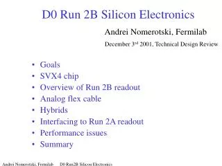
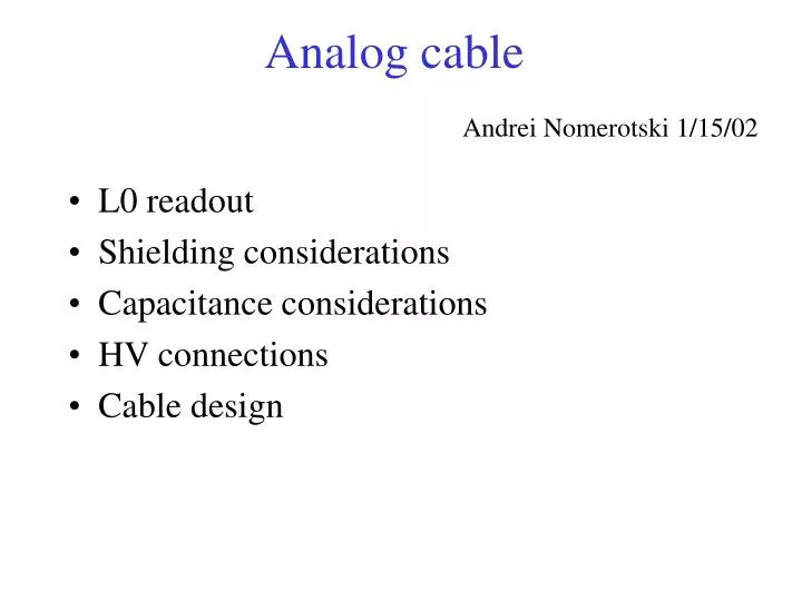
Analog cable. Andrei Nomerotski 1/15/02. L0 readout Shielding considerations Capacitance considerations HV connections Cable design. Layer 0 readout. twisted pair cable. digital cable. Junction Card. Layer 0. Shielding, GND. hybrid. analog cables. sensors. Shielding, GND.

E N D
Analog cable Andrei Nomerotski 1/15/02 • L0 readout • Shielding considerations • Capacitance considerations • HV connections • Cable design
Layer 0 readout twisted pair cable digital cable Junction Card Layer 0 Shielding, GND hybrid analog cables sensors Shielding, GND 6 pairs of analog cables 2 chip hybrids Common shielding
New design of analog cable silicon
Layer 0 noise S/N =10 C_silicon max C_cable Acceptable cable capacitance is determined by noise performance S/N = 10 after 15 fb-1 => total noise = 2200 => total capacitance < 33 pF => C_cable < 23 pF => C_cable <0.55 pF/cm for 42 cm long cable
Capacitance Calculations agree with measurements within 10% 50 mm thick substrate with er = 3.5 Settled on ~100 um pitch and 16 um trace width w/ ground shielding w/o ground shielding Red circles for 100 mm pitchBlue squares for 50 mm pitch 16 um => 0.32 pF/cm
Spacer between cables Epsilon = 0.7 * 1 + 0.3 * 3.5 = 1.75 Capacitance < 0.45 pF/cm
L0 connections HV HV (n+) HV GND Shielding SVX4 HV pad SVX4 GND GND HV (n+) • Metallization on n+ implant at the adge is used to route HV to HV pad • HV pad has a foil wrapped around the edge to the backplane • HV pad may also have a low pass filter
HV HV GND SVX4 SVX4 GND GND HV silicon
Analog cable design • Length 420 mm • Cable is symmetric left-right for the exception of “ears” • All distances are defined to centers of lines and pads • Bond pad size on signal traces is 150x60 um • “Ears” have fiducials in the center • HV trace has round shape at the ends 35000 um 15000 um 900 um HV trace, width 100 um 900 um 500 um 900 um 129 signal traces, width 16 um 13948 um 128 x 91 um GND trace, width 100 um 200 um 400 um 300 um 8000 um D 6000 um
HV trace 129 signal traces GND trace