Download
1 / 37
370 likes | 386 Views
Understanding the importance of RF filters in signal processing, including types like low-pass, high-pass, and band-stop filters. Learn about transmission line filters and design equations for different filter configurations.

E N D
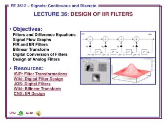
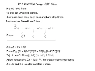
ECE 4990/5990 Design of RF Filters: Why we need filters • To filter out unwanted signals. • Low pass, high pass, band pass and band stop filters. Transmission Based Line Filters: Z Zin Y Zin = Z + 1/Y || Zin Zin = {Z + [Z2 + 4(Z/Y)]0.5}/2 = Z/2{1+ [1+4/(ZY)]0.5} Z=jwL, Y=sC Zin= (jwL/2) [1-{1-4/w2LC}0.5] At low frequencies, Zin = (L/C) 0.5, the characteristics impedance Zin = k, and this is called constant k filters.
As the frequency increases, the characteristic impedance becomes negative resulting in no energy transfer. The frequency at which [1-4/w2LC]=0 is called the cut off frequency, Wh= 2/[LC]0.5 This assumes infinite number of sections. But filters have finite sections. Difficult to control roll off and control the characteristics of the line. More sections, the better it is. L/2 L/2 L/2 L/2 L/2 L/2 C/2 C C C/2 Two Cascaded T sections
L/2 L/2 L/2 L/2 L/2 L/2 C C C Two Cascaded p sections Design Equations: Wh, cut off frequency, R is the characteristic impedance, C is the capacitance C=(2/wh)1/R , L=(2/wh)R R=50 ohms, wh= 500 MHz x2p = 3000 Mradians/sec C= (2/3000)1/50 = 2/150000= 13pf L= (2/3000)50 = 1/30 = 33 nH.
Low-pass m-derived filter using two cascaded T-sections • m-derived filter has a response generally attenuates more strongly as the cut off frequency w1 is approached. • The effect of Capacitance is reduced by adding a series inductor. L1/2 L1/2 L1/2 L1/2 L1/2 L1/2 2L2 L2 2L2 L2 C1/2 C1 C1 C1/2 Two Cascaded T sections
The cut-off frequency for a m derived section is given by w1 = 2(R/L1) /[4(L2/L1) +1] w1= 2m/[L1C1]0.5 R = [L1/C1]0.5 L2= (1-m2)R/2mw1 C1= (2m/w1)(1/R) L1 = (2m/w1)R
C2 C2 2C2 2C2 L1/2 L1 L1 L1/2 C1 C1 C1 C1=(2m/w1)1/R L1=(2m/w1)R C2= (1-m2)/2mw1R
Band Pass Filters C1 C1 L1 L1 L1 C1 2L2 2L2 L2 C2 C2/2 C2/2 L2 C2 L1= 2R/(w2-w1) C1= (w2-w1)/2wo2R C2= 2/R(w2-w1) L2= (w2-w1)R/2wo2
Filter Classifications and Specifications • Low Pass b) Band pass c) High Pass d) Band Stop (Band Eject) Parameters a) band width b) shape factor (skirt, selectivity) c) ripple. S6/60 = Dw60/Dw6 -6dB Dw6 -60dB Dw60 1 |H(jw)|2 Transition band 1/(1+e2) Passband Stopband 1/As2 wp ws
Butterworth Filters The Butterworth’s response magnitude as a function of frequency |H(jw)|2 = 1/[1+e2(w/wp)2n] Where the band edge wp is the frequency at which the power attenuation is (1+e2) The parameter n is the order(or degree) of the filter and it is equal to the number of independent energy storage elements as well as to the power of w with which the response magnitude finally rolls off. The 3-dB frequency wc is 1/[1+e2(wc/wp)2n] =1/2 wp=ewc The filter order can be determined depending by the attenuation in the stop band edge, 1/As2 = 1/[1+e2(ws/wp)2n] n= ln(As2-1)0.5/e/lnws/wp = ln (As/e)/ln(ws/wp)
Design of Filter We need to design a Butterworths filter with 1 db loss (0.794 gain) at the pass band edge of 1 GHz and require a 30 db attenuation at a 3 GHz stop band edge. • = [10 1dB/10 - 1] = 0.5088 For the stop band specification,A2 =1000, n = ln(9990.5/0.5088)/ln 3 = 3.76 n=4 bk = 2(e1/n)sin [(2k-1)p/2n] where k ranges from 0 to 1. k ranges from 1 to n, for k=1 b1= 2(0.50881/4) sin [(2-1)p/2x4] =2x0.844x0.3826 = 0.645. Lk= (R/wp) bk , L1 = R.b1/ 2pf = 50x0.645/(2x3.14x109) =5.135nH. Ck = bk/2pfR= 1x0.645/(2x3.14x109x50)= 2.0576 pF. L first C first L1= 5.1441nH C1= 2.0576pF C2=4.9675pF L2= 12.419nH L3= 12.419nH C3 = 4.9675 pF C4=2.0576pF L4 = 5.1441 nH
Low Pass Filter L first L1 L3 C4 C2
Band Pass Filters Butterworth type Bandstop Bandpass Low Pass High Pass (BW)L/wo2 1/(BW)L 1/woL L/BW L/wo BW/Lwo2 1/(BW)C BW/wo2C C/BW C/wo 1/woC Design a Band Pass Filter with BW=Df=100 MHz, fo=1GHz. BW=2p(f2-f1) fo=(f1f2)0.5 L1 L3 C4 C2 LPF
C3s L1s L1 L3 C2s L3s LPF L2s L4p C4 C2 C2p C4p L1= 5.1441nH C2=4.9675pF L3= 12.419nH C4=2.0576pF L1s = Lwo/BW = 5.1441x1e9/.1e9 =51.44nH C2s= BW/Lwo2 = 0.1/5.1x6.2x1e9 =e-10/5.1x6.2x6.2=3pf/6.2=0.5pf L3s= Lwo/BW = 12.419/0.1 = 124.1nH C3s= BW/Lwo2 = 0.1/12.41x(6.2)6.2x1e9 = 0.21pf C2p= C/BW = Cwo/BW = 4.97/.1 = 49.71pF. L2S= BW/wo2C= 0.1/(6.2 e9)5e-12x6.2e9 = 520 pH C4p= C/BW = Cwo/BW = 20.57pF L4p = BW/wo2C= 0.1/(6.2e9)2e-12x6.2e9= 1.3nH
Chebyshev Filters Mathematically, the Chebyshev response is of the form |H(jw)|2 = 1/[1 + e2Cn2((w/wp)] At w=wp, the |H(jw)|2 = 1/(1+e2) • is known as the ripple parameter and specified by the designer. The Chebyshev polynomial Cn(x) = 2x Cn-1(x) – Cn-2(x) Co=1 and C1 =x C2 = 2xC1-C0 = 2x2-1, C3 = 2x(2x2-1)-x=4x3-3x Another method of generating Chebeshev polynomial is in terms of some trignometric functions from which the oscillation between -1 and +1 (FOR |X|,1) Cn(x) = cos(ncos-1x) for |x|<1 For arguments larger than unity, Cn(x) = cosh(ncosh-1x) for |x|>1 x= cost, t=cos-1x y= cosnt , y = cos (ncos-1x)
The relationship between the stop band frequency ws, gainA(s)and order n is given by n = cosh-1([as2-1/e)/[cosh-1(ws/wp) = Cosh-1(As/e)/cosh-1(ws/wp) The Chebyshev is superior to Butterworth in the stop band. At high frequencies, a Butterworth with e=1 provides an attenuation |A(jw/wp)|2 = (w/wp)2n For Chebyshev, |A(jw/wp)|2 = 22n-2(w/wp)2n Computation of filter elements: b= sinh(tanh-1(1/(1+e2)0.5/n) The element values (normalized to 1 rps and 1 ohm) are then, c1=b/b Ck = bkbk-1/[ck-1 (b2+ {sin[(k-1)p/n]}2) bk= 2sin[(2n-1)p/2n]
Design of Chebyshev Low Pass Filters Normalized element values for 1.0dB ripple Chebyshev Low Pass filter C1(L1) = 2.024 L2(C2) = 0.994 C3(L3) = 2.024 Low pass filter design: Design a low pass filter with 1 dB pass band response, pass band edge at 1 GHz, stop band edge at 3 GHz, gain 30 dB. n=2.73 = 3 order. Lk= (R/wp) Ck , L1= 50x2.024/(6.2x1e9) = 16e-9 H= 16nH. Ck= Ck/6.2fR, C2= 0.994/6.2x1e9x50 = 3pf L3= 50x2.024/6.2x1e9 = 16nH. L3=16n L1=16n LPF C2=3pF
Design of Bandpass Chebyshev Filters 173fF L1=160 n L3=160n L3=16n 173fF L1=16n C2=30 pF LPF BPF L2=0.8nH C2=3pf C2= Cwo/BW= 3pf/0.1 =30pF L2 = BW/wo2C = 0.1/(6.2Xe9)2x3e-12 = 0.8nH. L/BW L/wo BW/Lwo2 C/wo BW/wo2C C/BW
Microstrip, stripline and Planar Passive Components General Characteristics of PC Boards: Metal thickness: I ounce of copper corresponds to 1.34 mil or (35 micron in thickness). 2 Oz(70 micron) and 0.5 Oz(17.5 micron) are also common thicknesses. The resistivity of bulk copper= 1.8 mW- cm and the corresponding sheet resistance is 0.5mW per square. The skin depth of copper = 2.1 mm at 1 GHz. And sheet resistance is about 8mohm per sq. Usually, the resistivity of film copper is higher than bulk copper by a factor of 2. The resistance depends on surface roughness, Fsr = 1 + 2/ptan-1[1.4(D/d)] where D is the surface roughness , d is the skin depth. Common Dielectric thicknesses are 1/32”(0.8mm), 1/16”(1.6mm)or 1/8 (3.2mm) In multilayer boards, the thickness of dielectric may be 1/64”. Most common PC board used at low frequencies is FR-4. The typical loss is 0.03dB/cm/GHz for 1/16”. The dielectric constant of FR- varies from 4.2 to 4.7 at 1 GHz. Suitable upto 5GHz.
Characteristics of PCBs The dielectric constant of PCB increases with increase in frequency –dispersion. The dielectric constant in FR-4 increases by 5% from 100 MHz to 5 GHz. Other materials are from Rogers Corporation. In addition, for high performance one can use saphire, allumina, beryllia and quartz. Transmission lines on PC Boards W W T T H H Microstrip Stripline The charactersitics of strip line: 1) Stripline is nearly self shielding: minimizes couling and radiation losses. 2) TEM propogation Disadvantage: Making connections to center conductor. The Charactersitic Impedance of stripline, Zo=( 60/er )ln[6H/pW(0.8+T/W)}
The above formula is valid for narrow lines: i.e. lines defined by W/(H-T),0.35 for a total dielectric thickness of 1/8” using 1 Oz copper, a 50 ohm line requires a conductor of approximately 1.25mm. For more accurate Zo is given by Cohn’s expression Zo = hK(k)/[4(er)0.5 K’(k)] where k =[cosh(pW/2H)] -1 • is the impedance of free space, = (mo/eo)0.5=120p K’(k) /K(k) = {1/p ln(2(1+k’0.5)/(1-k’0.5)] for 0<k<0.7070 {1/p ln(2(1+k0.5)/(1-k0.5)] for 0.7070<k<1 and k’ = (1-k2)0.5 Equations for Microstrips For microstrips, Zo = (mrmo/ereo)0.5 (H/W)[ 1+1.735er-0.0724(W/H) -.836] -1 If the thicknesses of the metals are included,replace W by Weff= W+T/p[ln(2H/T) +1] Disadvantages: • Energy is delivered to substrates leading to loss if the substrate is dissipative. • Ground plane is not easily accessible.
Line-To-Line Discontinuities Discontinues in the transmission Line can result higher excitation Modes. H/2 W H/2 Ceq= e(WH/2 + H2/4)/H =e (W/2 + H/4) Zo The effective length extension Dl is given by, Dl/H = 0.412(ere + 0.3)(W/H +0.262)/(ere-0.258)(W/H+0.813) ere, effective realtive dielectric constant= (er +1)/2 + (er-1)(1/2)(1+10H/W) -0.5 Excess capacitance due to sharp bend. Use Chamfered bend. For a right angle bend 1.8W area.
Coplanar Waveguide (CPW) and Coplanar Strip W W w S S Advantages of Coplanar Structures: a) Both ground and signal lines are accessible from the top surface. Probing is easy. b) Less loss. The characteristic impedance impedance Zo= hK’(k)/[4(ee)0.5K(k)] for CPW = hK’(k)/[(ee)0.5K’(k)] for CPS k = S/2/[S/2 +W} ee= 1 + (er-1)/2 K’(k) K(k1)/K(k)K’(k1) In turn, k1 = sinh(pS/4H)/sinh(p{S/2 +W}/2H) K’(k) /K(k) = {1/p ln(2(1+k’0.5)/(1-k’0.5)] for 0<k<0.7070 {1/p ln(2(1+k0.5)/(1-k0.5)] for 0.7070<k<1 and k’ = (1-k2)0.
Line Discontinuities W2 b= 0.4[W12+W22]0.5 b W1 q =tan-1(W1/w2) Circular bend with radius greater than 3 times the width. The capacitance discontinuity: (W2-W1)l l W1 W1 W2 l Tapered transition can be used to reduce the energy stored due to higher order modes. Inductive notched line.
Line Discontinuities Effects: The inductance due to discontiuity, L= lZo,n(er,eff,n)0.5[1-(Zo,w/Z0,n)2]/c Where the subscripts n,w stand and wide, respectively. T Junction Shortening: The shortening (due to capacitive coupling)occurs at the junction of a wide and narrow line. Dl/H = 120p/Zl(ere,ser)[0.5-0.16(Z1/Z2)(1-2ln[Z1/Z2])] Z1 Transitions between connectors and transmission lines Z2
Passives made from Transmission line Segments Z(l)/Zo = (ZLn + jtanbl)/{1+jZLntanbl} where Zln is the normalized load impedance Where b is an imaginary part of the propogation constant, g b=Im[g] = w[LC]0.5=w/v er,eff = {1+0.63(er-1)(W/H)0.1255 for W/H>0.6 {1+0.63(er-1)(W/H)0.1255 forW/H<0.6 For a 50 ohm line on FR4, W/H=2 and the effective dielectric constant is about 3.5(if the actual bulk er=4.5). If the load impedance goes to infinity, Z= Zo/jbl = Zo/jw(l/v) The capacitance is therefore, C=l/vZo= l(er,eff)0.5/cZo The time constant Zoc is simply the one-way time of flight. FR-4 offers a capacitance of 2.5pF/cm2. A short segment terminated in a short circuit will appear inductive since we have a Current loop. Z=Zo bl = lZo(er,eff)0.5/c The line dimensions of components must be smaller than wavelength.
Resonators Input Impedance of a line that is l/4 in extent: The impedance =infinity. If the length is greater than l/4, the impedance is capacitive. If the length is less than l/4, the impedance is inductive. The ‘Q’ of the resonator = inductive or capacitive reactance/real part of impedance Z(l)/Zo = (Zln +tanhgl)/(1 +Zln tanhgl) =1/tangl =1/tanh(a+jb)l If al<<1, input resistance, Reff= Zoal= Zo(al/4) L= Q = woL/Reff =
Combiners Combiners are used to combine signals from multiple sources to create a single output. They can also be used as power splitters. Resistive Splitter/combiner: V1 V1 Zo/3 3Zo 3Zo Zo/3 Vin Vin 3Zo Zo/3 2Zo V2 Distributed Combiners: V2 2Zo Zo Zo 2Zo 2Zo
Zo l/4 Z Z0 R l/4 Zo Z
Hybrids and Baluns Classic telephone Hybrid Port3 Through Output Input line A C Port1 Port2 Isolated output R D Auxiliary(coupled) output B talk listen Through Input Isolated Coupled Symbols for hybrid couplers
C(null ouptput) Zo B, Output1, Zo Circumference of the circle is 3l/2. S Input signal at A, when enters the hybrid, at point B, the clockwise signal traverses l/4and anticlockwise, and conuter clockwise 5l/4(3l/2-l/4) Therefore signals add up. Input A, Zo D Zo, D Output2 Ring (or rat race ) hybrid
Lumped 180 Splitter/combiner If Zo is the source resistance driving the input port, the input impedance of each filter is 2Zo. ZL is the load impedance from each output to ground, The characteristic impedance of each arm is given by (L/C)0.5 = (2ZoZL)0.5 (L/C) = 2ZoZL wo = 1/(LC)0.5 C = 1/(wo)(2ZoZL)0.5 L = (2ZoZL)0.5/wo Vlag L C 2ZL C Vin C C Vlead L For a 1 GHz hybrid driven by 50 ohm, and terminated in 100 ohm, 50 ohm from each output to ground, the component values are about 11.3nH and 2.25 pF.
Lumped Coupler l/4 sections are replaced by low pass p sections and l/2 sections are replaced by high pass T network. B C L1 C1 C1 C1 C1 L1 L1 C1 C1 A D C1 C1 If all the inductors and capacitors are equal, the ring impedance at the center frequency of operation: C1= 1/(woZo20.5) and L1=Zo20.5/wo Lumped versions have the same narrow bandwidth (10 to 15%) as the distributed versions.
Branch Line Hybrid A(input) Zo Zo B(output 1) Zo/20.5 l/4 Zo Zo D(output 2) C(isolated) Zo/20.5 Zo Zo l/4 Branch line hybrids are used to generate(or combine) two signals that are in quadrature rather than in antiphase with each other. Zs Zs Zo Zo Zo Zo B, (output 1) A(input) B, (output 1) A(input) Zp Zp Zp Zp Common mode D,(output 2) C(isolated) Zo Zs Zo
Lumped implementation of 90 hybrid C L1 C2 C1 C2 C1 L2 L2 C2 C2 A D L1 C1 C1 C L1 C2 C2+ C1 C1+ L2 L2 C2+C1 A D L1 C1+C2
Directional Couplers Directional couplers are four port devices capable of splitting power by prescribed amounts that generally differ considerably from 1:1. They are used for feed back in power amplifiers They are used to resolve forward and reverse signals. Figures of merit for a directional coupler include coupling factor, isolation and directivity. The coupling factor is defined as the ratio of input power to the power delivered to the coupled (auxiliary) port. CF = PIn/PAux|forward Typical coupling factor is from 3dB to 20 dB. If the directional is operated in reverse, with power now supplied to the through output with input terminated, some power leaks to the auxiliary port. A measure of how well the reverse leakage is suppressed is the isolation factor. I= Pin/Paux |reverse Isolation factors of 30-60 dB are not uncommon for commercially available units. The directivity D = I/CF= Paux|forward/Paux|reverse