Download

1 / 5
60 likes | 97 Views
For the better functioning of prototyping systems, PCBs are made in this way. This is an important piece of information, which would allow you to take firm decisions regarding any Printed Circuit Board

E N D
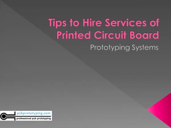
Printed Circuit Board – Everything That You Need to Understand Prototyping system
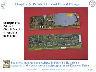
Since the IT sector is developing every day, there is a dire need for the advancement of technologies. Old technologies are no longer and people crave for new ones. Before PCB came into existence, engineers or software developers mainly used technologies like wire wrapping and soldering from one point to the other. These took a lot of precious time and were very faulty. That is the reason why PCB or better known as Printed Circuit Boards came into use for advanced prototyping. • PCB is a widely used product. It is mainly made up of Copper, Substrate, Silkscreen, and Solder Mask. However, if it is placed in the order of how it remains inside the PCB, it is Substrate, Copper, Solder mask, and Silkscreen. Modern-day PCB is very different from the ones that were used earlier. In the very beginning, PCB used leaded substances. Later, wave soldering was introduced in order to lessen the time it took. In Modern Day PCBs, no holes need to be dug in order to make the PCB function smoothly.
PCB as Prototyping system helps in better wiring plans and soldering. Modern-day PCBs are made in the following way – • For the four layers of PCB, a separate film is generated or produced. This is done using the mechanisms of computer software. • The copper clad board which is one of the most important components of PCB is cut into the required dimensions in order to support the prototyping well. • Carbide drills are used which drills and create holes. • There must be a secured connection between two or more sides of the board. Therefore, a thin copper deposit is used to trace a good connection between all the sides of the board. • In order to create a negative image, the board is exposed with the help of a film and a light source. You need a photosensitive plate in this particular process.
PCB as Prototyping system helps in better wiring plans and soldering. Modern-day PCBs are made in the following way – • In this, tin is used in the surface after the process of adding copper in the holes. • The dry or unused film is gradually removed. The tin on the surface protects the copper from being removed while performing this process. • Now, the solder mask needs to be applied throughout the board. • The solder pads which had been used earlier are provided with a solder coating again. Gradually, the circuit board is taken out of the tank. • You might or might not use the screen printing process.
For the better functioning of prototyping systems, PCBs are made in this way. This is an important piece of information, which would allow you to take firm decisions regarding any Printed Circuit Board.