Download
1 / 11
0 likes | 80 Views
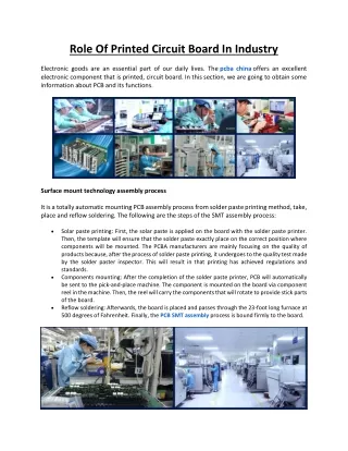
Printed Circuit Boards (PCBs) are essential components in electronic devices, providing the foundation for mounting and connecting electronic components through conductive pathways, enabling efficient signal transmission and functionality in various applications from consumer electronics to industrial equipment.

E N D
A BASIC INTRODUCTION FOR DESIGNING A PRINTED CIRCUIT BOARD (PCB) www.pcbcircuit.in
Content INTRODUCTION 01 02 PCB Design Software 03 • Initial Design Steps 04 • PCB Layout Design 05 • Routing Traces 06 • Design Rules and Checks 07 • Generating Gerber Files 08 • Prototyping and Testing
Printed Circuit Boards (PCBs) are essential components in electronic devices, providing the foundation for mounting and connecting electronic components through conductive pathways, enabling efficient signal transmission and functionality in various applications from consumer electronics to industrial equipment.
PCB Design Software • Key Features • PCB design software, such as Eagle, Altium, and KiCad, facilitates creating circuit diagrams and layouts. These tools offer features like component libraries, design rule checks, and multi-layer support, streamlining the PCB design and manufacturing process. USER-FRIENDLY INTERFACE • 01 • COMPONENT • LIBRARIES • 02 • DESIGN RULE • CHECKS. • 03
Initial Design Steps SCHEMATIC CAPTURE - Creating a circuit diagram using design software. - Selecting components from libraries. COMPONENT PLACEMENT - Arranging components logically and efficiently on the schematic.
Board Outline • Component Placement PCB Layout Design - Positioning components on the board considering accessibility and heat dissipation. - Defining the size and shape of the PCB.
ROUTING TRACES Trace Routing Layer Management • Connecting components with copper traces. • Avoiding trace overlap and crossing. • Using multiple layers for complex designs, including power and ground planes.
Design Rules and Checks • 1. Design Rule Check (DRC): • Ensuring compliance with manufacturing specifications. 2. Electrical Rule Check (ERC): • Verifying electrical integrity and connections.
Generating Gerber Files • GENERATING GERBER FILES • Creating Gerber files for manufacturing. • Including drill files and Bill of Materials (BOM).
Prototyping and Testing • 1. Prototyping: • Ordering a prototype to test the design. • 2. Testing and Validation: • Verifying functionality and performance. • Making necessary adjustments based on test results.
THANK YOU +91 9306218403 www.pcbcircuit.in