Download
1 / 1
10 likes | 112 Views
Jason Allen Florida A&M University. Low Power T/R Switch for NMR Application. Introduction :

E N D
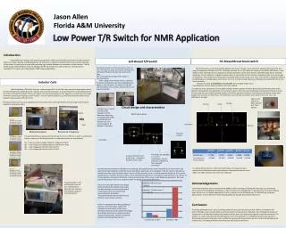
Jason Allen Florida A&M University Low Power T/R Switch for NMR Application • Introduction: • Transmit/Receive switches, also known as transceivers, allow both transmitter and receiver to share the same antenna or probe. Typically, in NMR applications T/R switches are required to reliably perform the switching operation of high power RF signals at a fast rate while providing high isolation between the transmitter and the receiver. The Pin diodes used in these switches can be self biased by the RF signal itself or an external DC bias. The T/R switches presented in this poster were developed for NMR mapping applications. DC-Biased Broad band switch Self-Biased T/R Switch Considerable amount of time during the course of this internship was spent learning the workings of a self biased T/R switch like the one show on the right. The circuit and the workings of the switch is illustrated below. After taking measurements of the resonance frequencies of inductor coils the modifying process began on the T/R switch. The switch on the right was modified to have a similar characteristics as the switch on the left. The Requirements for the DC-Biased Broadband-switch was to create a low-powered dc-biased switch, that works for a range of frequencies 300MHz to 1.1GHz. The diodes selected for our T/R switch are surface mount HSMP-3892 diodes. These diodes are fast switching, has low capacitance, and low impedance, these characteristics made them Ideal for the switching application. The Xc (capacitor’s impedance) value had to be low and the XL (the Inductor’s Impedance) had to be much larger in comparison. The Capacitors are being used as dc-blocks and only need to be 1 or 2 ohms. The Inductor’s impedance needs to be high because it is being used as an AC-block, and it has to block the high frequencies. 500ohms was selected for the XL and 2ohms for the Xc. Using the formulas: C=(1/(2πfXc)) and L=(XL/2πf), the calculated ranges were; Capacitance: 61.21pF to 265pF, Inductance: 61.2nH to 265nH. Inductor Coils Before designing a T/R switch there are a few concepts of RF circuits that I was required to understand, such as resonance frequencies, quality factor etc. Inductor coils have self-resonances at certain frequencies which depend on the size of your coils and the number of turns per length. The resonance frequency is the frequency in which the coil provides minimum resistance and maximum power transfer. A vector network analyzer is a useful instrument that allows you to measure various aspects of the RF circuit. Prototype surface coils in various configurations shown below were used to get familiar with the usage of the network analyzer to characterize them. The capacitor value selected for this was 68pF. Utilizing a known capacitor we were able to calculate the Inductance of the different coils tested for this application. The inductance values of the coils were obtained by connecting the inductors across a known capacitor and using the network analyzer to find the resonance frequency. From this point the known values were plugged into a formula L= (1/(4π²f²C)). The Inductance value selected was 150nH, which came in form of a 7 turn coil illustrated to the right. Figure to the right is the 68pF capacitor and 7turn inductor DC Bias DC Bias Probe Circuit design and characteristics LC Tank circuit, in which provides a high impedance at the Resonance frequency, consisting of the diodes in parallel with the Inductor coil. This prevents against RF leakage in the diodes Output NMR Probe/ Antenna 2 turn #2 146.39MHz @-14.503dB 640.01MHz @-3.572dB 851.19MHz @-26.72dB S## Transmitter Input Receiver Network Analyzer Resonance Frequency Receiver/ preamp 2 turn #1 141.78MHz @-0.7029dB 424.60MHz @-2.540dB 651.30MHz @-16.017dB 850.64MHz @-16.017dB This particular Network Analyzer consist of 2 ports; Port 1 and Port 2. In order to understand how to connect your device to the port it is important to know the S-parameters. S11 – Is the input port voltage reflection coefficient at Port1. S22 – Is the output port voltage reflection coefficient at Port2 S12 – Is the voltage gain (transmission) at Port1. S21 – Is the voltage gain (transmission) at Port2. Transmitter 2 Turn Coils in Parallel 130.26MHz @-2.029dB 143.80MHz @-9.005dB 819.84MHz @-6.501dB 1.000GHz @-11.078db The diodes are packaged in a “series” configuration, but the leads were soldered to form a parallel connection ¼ wave transmission line is used as an impedance Transformer @ 1.1GHz. To improve the isolation at 1.1GHz, the original silver-mica capacitors were replaced by multilayered-ceramic-chip-capacitors. Although the insertion loss is higher, the added isolation was much more important. During Transmission both sets of diodes are conducting. Utilizing the quarter wave transmission line, the transmit side experiences high impedance, while the receive side ideally experiences zero impedance. Thus the current is directed up towards the probe, away from the transmit section of the transmission line. In receive mode the diodes are all in reverse-biased position, therefore they act as open circuits and allow the signal from the probe to travel directly to the receiver. As for the inductor connected to the diodes in the transmit portion of the circuit, it adds additional impedance. This helps prevent the diodes, which act as capacitors when not biased, from leaking RF Energy. 4 turn Coil 80.03MHz @-5.96dB 349.54MHz @ -1.523dB 632.25MHz @-4.160dB 794.37MHz @-9.663dB 989.82MHz @-13.127dB The photograph on the left illustrates how the S11 measurement is done with the inductive loop utilizing using the network analyzer Acknowledgements I would like to take this time to thank all of the NHMFL staff for assisting me during this internship. To Jose Sanchez, thank you for accommodating and helping to make this experience unforgettable. I truly appreciate the chance of being a part of this once in a lifetime opportunity. Thanks to everyone in the RF laboratories, Dr. William Brey and group. Special thanks to Kiran Shetty for mentoring and guiding me through this research experience. The chart to the right compares the design with and without the inductor. Based upon the data received, the switch performed at it’s best when the 2 turn Inductor was connected across the diodes. The graph illustrates the Insertion loss and isolation values of both scenarios. Conclusion: The design ultimately was a success, providing isolation at the 5 key frequencies, which makes it a broadband T/R switch. Although it was a success there are still many facets to improve upon. Hopefully later changing the location of components on the board and placing the inductors further apart may help prevent against unwanted resonances. The isolation at 1.1GHz was improved by switching from silver-mica capacitors to multilayered ceramic chip capacitors. Eliminating the coaxial transmission lines and directly mounting the RF connectors on the PC board should improve the insertion loss. I’m looking forward to improving upon this design in the future. In the Red the graph shows that by adding an inductor across the diodes it adds more impedance to that section of the circuit, therefore helping to prevent against RF leakage from diodes, which act as capacitors while in reverse biased position, therefore increasing isolation and lowering insertion loss.