3D Technology Developments in Europe and EU Supported Activities
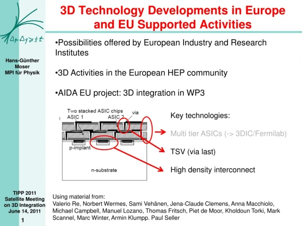
3D Technology Developments in Europe and EU Supported Activities. Possibilities offered by European Industry and Research Institutes 3D Activities in the European HEP community AIDA EU project: 3D integration in WP3. Key technologies: Multi tier ASICs (-> 3DIC/ Fermilab ) TSV (via last)

3D Technology Developments in Europe and EU Supported Activities
E N D
Presentation Transcript
3D Technology Developments in Europe and EU Supported Activities • Possibilities offered by European Industry and Research Institutes • 3D Activities in the European HEP community • AIDA EU project: 3D integration in WP3 Key technologies: Multi tier ASICs (-> 3DIC/Fermilab) TSV (via last) High density interconnect Using material from: Valerio Re, Norbert Wermes, Sami Vehänen, Jena-Claude Clemens, Anna Macchiolo, Michael Campbell, Manuel Lozano, Thomas Fritsch, Piet de Moor, Kholdoun Torki, Mark Scannel, Marc Winter, Armin Klumpp. Paul Seller
Possibilities offered by European Industry and Research Institutes VTT Frauenhofer IZM IMEC Frauenhofer EMFT CEA LETI (CMP) CNM Information from an AIDA WP3 workshop in May This is not necessarily complete (Sintef? FBK? CNM, ST?)
CEA LETI Open 3D initiative: 3D technology service for research organizations and industry cost effective based on mature technology customization possible TSV Solder pillars Solder bumps
Fraunhofer EMFT • SLID interconnection replacing solder bumps • Small pitch (limited by alingments precision of flip chip) • Stacking possible • Pitch < 20 µm in view • ICV (Inter Chip Vias) • Tungsten filled vias • Aspect ration: 8:1 • VIA diameter > 2 µm • 0.3 Ohm for 2x2x20µm³ • Handling concept for thinned ASICs
Fraunhofer IZM Experience with bump bonding for ATLAS, MEDIPIX, SLAC Pitch ~ 50 µm Tapered VIAs (copper lined) ~ 50 – 100 µm New facility for 3D in Dresden (300 inch wafer)
IMEC TSV – via last (post processing) Chip backside to metal 1 Pitch: 40 µm Via diameter: 25 µm Thickness: 50 µm (2:1) TSV – via middle (part of CMOS process) Connections to metal 1 Pitch: 10 µm Via diameter: 5 µm Thickness: 20 µm Integrated in IMEC’s 130nm CMOS line Interconnection: In or CuSn microbumps Pitch: 20 µm (10 µm in development)
Activities by European HEP Institutes UK (RAL) Germany Bonn MPP France IPHC CNRS CERN Italy (INFN) Furthermore: Interest by XFEL community
ITALY • Pixel sensor for superB • Superpix 1: 2-tier version of a readout chip for hybrid pixels • APSEL: 3D CMOS MAPS sensors in DNW technology First versions in production (Fermilab 3D iC) Will submit improved versions in the next CNP/MOSIS/Tezzaron run Strong interest in interconnection of tiers (sensor/readout) in heterogeneous technologies (via last) (-> AIDA)
France CPPM: ATLAS FE_I4proto chip “translation” in 3D (with Bonn, LBL) 6.4 mm FE_TC4 Analog C1 3*4 mm FE_TC4 Analog C1 3*4 mm FE_TC4 Digital simple C2 3*4 mm FE_TC4 Digital upgraded C3 3*4 mm 5.5 mm Test zone 6.4*1.4 Test zone 6.4*1.4 IPHC: 3D visio 10/02/2009
MPI Munich: 3D interconnection for sLHC 3D demonstrator (aimed for ATLAS pixel upgrade) Based on ATLAS FEI3 chip Thin sensors made at MPI HLL SLID interconnection by EMFT TSV by EMFT 1st step: SLID only (no TSV) Successful (however, problems with alignment & interconnection yield in some chips) 2nd step: SLID & TSV Trials on dummy FEI3 wafer Next: full process on hot wafers & sensors
Bonn University: An ATLAS pixel module concept with TSV • Similarto MPI project, in collaborationwith IZM • useverythin (~100 µm) FE-I4 (2x2 cm2) chips • use TSV fortheroutingofsignals on thechipbackside • An ATLAS pixelmodulewith90µm thick FE-I2andtapered TSVs isbeingbuilt @ IZM Berlin • First structuresarrive 13.6.2011 • Furthermore Bonn joinedtheFermilab 3DIC project (3D versionof FEI4) Tapered side walls TSV Backside redistribution
CERN Medipix 3 chip is ‘3D friendly’ => back side connectivity TSV landing pads in periphery No filling structures in TSV area! Wafers exist, looking for TSV service TIMEPIX 3 will have similar features
Detector eg. CZT Wire bond Gold studs 50um analogueASIC SLID Bonds Thick digital ASIC Heat sink PCB UK: RAL • 3D version of an x-ray imager for CZT sensors • Based on HEXITEC 8080 chip • Specifically a 3D-ASIC:- with two 2-D active layers bonded together at many points on surface • Layer 1:- Analogue preamplifiers • Layer 2:- Digital ADCs • 40 x 40 pixel, 250 µm pitch • Progress this year. • Define a Back-End-of-Line Process with EMFT so we could use different CMOS processes on the different layers. Cu/Sn SLID process with W vias. • RAL has designed and built the 2 layer CMOSwafers for EMFT bonding 3D-IC Upper pixel 4040 pixel ASIC 3D-IC Lower pixel
EU Supported Projects Project officially started February 1st 2011 Budget: 26 M€ with 8 M€ from EU over 4 years
WP 3:3D interconnection The aim is to build a demonstrator of a 3D vertically integrated pixel sensor, which provides a tool to qualify the technologies that are involved in 3D integration and makes them accessible to the community. WP3 plans to follow a “via last ” approach to 3D integration to build a 2-layer device in heterogeneous technologies, where the two layers are fabricated independently, and TSVs (Through Silicon Vias) and interconnections are made as the last steps of the process. Budget: ~ 800 k€ (EU contribution) 17
Program & Institutes Participants: CERN, CEA, CNRS, MPG-MPP, UBONN, INFN, AGH-UST, CISC, UB, UU, STFC Associates: IPASCR, NTUA, UNIGLA, UNILIV, FOM 18
Sensors Options for dedicated sensors FBK (Trento, Italy) Planar pixels, full-”3D” pixels with slim edge; active edge sensors also being developed VTT (Finland) Edgeless detectors, R&D towards 4-side buttable devices (TSVs, flip-chip bonding) MPI-HLL (Munich) Thin pixel sensors with UBM (copper on Ti/W) IMB-CNM (Barcelona) Active edge, “3D“ pixels, bump bonding (UBM and bump growing) 19
CMOS readout circuits for 3D integration • Possible Manufacturers: • IBM (via CERN),IBM (via MOSIS), Chartered (via Equipic), Tezzaron/Chartered 3D (via CMP/CMC/MOSIS), UMC, AMS (via EUROPRACTICE), others • Possible selection criteria: • CMOS technology node (350nm, 250nm, 130nm, 90nm…) • Full wafer access (postprocessing for 3D interconnection) • Possible via CERN (IBM) or CMP(?) • Other possibility: use/modify existing chip (e.g. MEDIPIX3) 20
Post processing and interconnection • Workshop in Bergamo (May 23): • Contributions from: • CAE LETI • CMP • Fraunhofer EMFT • Fraunhofer IZM • IMEC • T-Micro • VTT Maturity (service or R&D) Projection - Fine pitch, via density Plan: select process best adapted for AIDA WP3 goals within the next 6 months 21
Conclusions • European industry and research institutes offer various processes for 3D integration • Shift form basic R&D to ‘service’ • Mainly via last processing (but via middle offered by IMEC) • ‘mature process’ offer rather modest pitch (vias & interconnects) • Fine pitch/hight aspect ration still in R&D stage, but demonstrators being built • Several R&D projects for HEP by European groups: • Mainly for sLHC, ILC, super B-factories • Groups outside HEP show interest (Medipix, x-ray imagers) • EU funded AIDA project explicitly addresses 3D integration • WP3 will be a common platform to bundle and advance the diverse 3D activities in Europe • Emphasis is on heterogeneous technologies (via last), complementary to Fermilabs 3DIC
Europe has 3D structures, too (and much older ones) From Valerio Re – VIPS2010 in Pavia