Download
1 / 13
130 likes | 289 Views
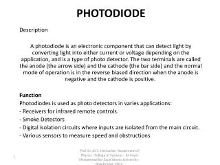
Advanced Photodiode Development 7 April, 2000 James A. Burns jab@ ll.mit.edu. 3D Photodiode Development Snapshot. Goal Produce high quality photodiodes for visible imaging Standard CMOS processes do not produce image-quality photodiodes

E N D
Advanced Photodiode Development 7 April, 2000 James A. Burns jab@ ll.mit.edu
3D Photodiode DevelopmentSnapshot • Goal • Produce high quality photodiodes for visible imaging • Standard CMOS processes do not produce image-quality photodiodes • Photodiode process must be compatible with 3D integration • Approach • Review existing Lincoln silicon-photodiode processes • Optimize an existing process to meet the active pixel sensor requirements using • Process and device simulation • Additional characterization of existing photodiodes • Tasks • Define photodiode requirements • Define photodiode fabrication process • Layout a photodiode test chip • Fabricate and characterize photodiodes • 3 runs to optimize device properties • 3D integration and photodiode characterization
Lincoln Silicon Photodiode Survey • A comparison of photodiodes and the principal processes which affect dark current
Photodiode Process1st Pass • Bulk substrate • 25-mm epi, 300 -cm • 0.01 -cm p-type wafer • Process highlights • LOCOS isolation • 30-nm stress-relief oxide • 20-nm Si3N4 • 250-nm field oxide • Dual N+ implant • Phosphorus to obtain a deep junction • Arsenic to maintain high C0 • Extended anneal to repair N+ implant damage • Eight Mask Levels • Six through metal-1, passivation • Deep via and back metal for 3D integration tests
Photodiode Simulations Xj 0.5 mm Field Oxide P-type epi Profile following field oxidation LOCOS bird’s beak limits fill factor Completed simulation indicates a 1-mm junction depth
Photodiode Test Chip Characterization • Front side measurements • Diode leakage vs diode area, perimeter • Cross talk vs diode, isolation spacing • Diode responsivity(l,F), dark current, linearity(l,F) • Array uniformity and yield • Back side measurements • Determine if bond process degrades photodiode • Measure photodiode properties vs silicon thickness • 3D imager • Measure photodiode properties vs deep via resistance • Determine whether 3D assembly degrades photodiode • Deep via and back metal layers included in reticle set
Imager Test DevicesDiode Array Metal-1 N+P Diodes P+ Contacts • Array measurements • Leakage and cross talk vs diode area and N+N+, N+P+ spacing • Responsivity, linearity, and yield
Imager test DevicesEdge Effects Diode N+P Outer Diodes-2 in parallel P+ Contact N+P Diodes-5 in parallel • Measure leakage vs diode area, perimeter to isolate edge effects • LOCOS-induced stress, inadequate channel stop • Misaligned contacts
Imager Test DevicesIndividual Diodes • Measure leakage vs isolation features P+ Contact N+P Diode N+-N+ Gap
Imager test DevicesParasitic FET o N+P Diode G L g P+ Contact W Metal-1 Gate • Characterize leakage mechanisms • separate surface from bulk leakage with metal gate • determine minimum N+ separation
Backside Illuminated Characterization Photodiode wafer Support wafer Support wafer Completed backside imager Metal-1 • Photodiode wafer bonded to support wafer • Silicon thinned • Silicon etched to expose metal-1 pads • Standard CCD process for backside imaging F(l) + Silicon N+ Silicon Bond layer Oxide Support wafer
3D Assembly Characterization F(l) Photodiode wafer + Transfer wafer Support wafer Completed backside imager Photodiode wafer • Photodiode wafer bonded to oxidized silicon wafer • Silicon removed from transfer wafer • Deep vias etched and connections made to metal-1 of photodiode wafer • Assembly bonded to support wafer • Silicon thinned • Silicon etched to expose metal-1 pads
Photodiode Development Status • Silicon photodiode process survey complete • Initial process defined; optimization via simulation underway • Test devices defined; layout nearly complete