Morphological Evolution in Graphene Formation on SiC(0001)
Explore the formation of graphene on silicon carbide, revealing morphological changes at different temperatures. AFM images depict graphene characteristics and mechanism insights.

Morphological Evolution in Graphene Formation on SiC(0001)
E N D
Presentation Transcript
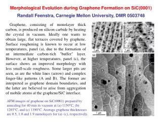
Morphological Evolution during Graphene Formation on SiC(0001) Randall Feenstra, Carnegie Mellon University, DMR 0503748 Graphene, consisting of monolayer thick carbon, is produced on silicon carbide by heating the crystal in vacuum. Ideally one wants to obtain large, flat terraces covered by graphene. Surface roughening is known to occur at low temperatures, panel (a), due to the formation of an intermediate carbon-rich "buffer" layer. However, at higher temperatures, panel (c), the surface shows an improved morphology with less small-scale roughness. Some larger pits are seen, as are the white lines (arrow) and complex finger-like patterns (A and B). The former are interpreted as graphene domain boundaries, and the latter are believed to arise from aggregation of mobile atoms at the graphene/SiC interface. AFM images of graphene on SiC(0001) prepared by annealing for 40 min in vacuum at (a) 1150C, (b) 1285C, and (c) 1390C. Average graphene thicknesses are 0.5, 1.0 and 1.9 monolayers for (a)–(c), respectively.
(a) (b) Transport Measurements in the LUMO band of Pentacene FilmsRandall Feenstra, Carnegie Mellon University, DMR 0503748 Pentacene films have been prepared on silicon carbide substrates by deposition in vacuum. Using a scanning tunneling microscope, current is injected into the HOMO and LUMO bands (negative and positive voltages on the plot). In the latter case, saturation of the current is found at a current of about 20 pA. This saturation arises directly from limited transport of the electrons in the LUMO band. The corresponding mobility is found to be 6×10⁻⁶ cm2/V s, a very low value that is not directly accessible by conventional measurements (using deposited contacts). Such a low mobility implies the formation of a self-trapped polaron, and similar effects are known to occur in other molecules. Our technique provides a means of probing those systems. (a) AFM image of pentacene on SiC, showing layered morphology. (b) Tunneling current vs. voltage, obtained at different tip-sample separations s.
Lecture to local High School Calculus class on Applications of Mathematics in PhysicsRandall Feenstra, Carnegie Mellon University, DMR 0503748 In a calculus class at the Fox Chapel Area High School in Pittsburgh, Prof. Feenstra gave a lecture on applications of mathematics. The students in the class had learned about calculus all semester, and the question arose of “who uses this stuff.” To answer this, Prof. Feenstra discussed the use of calculus in physics. The lecture progressed from a derivation of the differential equation describing spring motion to a discussion of electric and magnetic fields and electro-magnetic waves. Demonstrations included weights on springs, the magnetic field of a bar magnet, and computer visualization of vector summation of fields.


