Download
1 / 5
50 likes | 297 Views
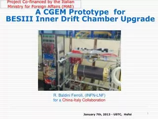
pALPIDE-fs HIC prototype requirements WP6 – 30.1.2014. pALPIDEfs chips for HIC assembly. Wafer processing steps (pad wafers+real wafers): Ni/Au metallisation Thinning and dicing Pad wafers: from TJ (identical layout as real chips) picture

E N D
pALPIDEfs chips for HIC assembly Wafer processing steps (pad wafers+real wafers): Ni/Au metallisation Thinning and dicing Pad wafers: from TJ (identical layout as real chips) picture Send 2 wafers for thinning and dicing to provide first components (50 um thick and 450 um thick) Send one further wafer for Ni/Au metallisation (ENIG) next week, followed by thinning and dicing Real wafers: Wafer delivery from TJ foreseen ~end March 2014 (tbc) Followed by thinning and dicing First real pALPIDEfs chips available ~ mid April 2014 No yield information at this point! WP6, 301.1.2014, P. Riedler
Pad layout Information provided by G. Aglieri Requires new FPC and ceramic grid! 24 16 16 16 31 103 contacts WP6, 301.1.2014, P. Riedler
Pad geometry Information provided by G. Aglieri Square Al contact pads (224 um x 224 um) “Quasi-round” opening in the passivation (200 um “diameter”) WP6, 301.1.2014, P. Riedler
Thinning and dicing, timeline Thinning and dicing: Thickness 50 um (+/- 5 um) – as up to now Dimensional precision should not exeed +20 um – new requirement, needs to be confirmed on first samples back Time line: ~end Feb: first thin chips with Al pads available ~beginning of March (tbc): ~ first Ni/Au plated thin chips available