PRR on Patch-Panel ASIC 9 Dec. 2002 KEK SOS
230 likes | 345 Views
This document presents a comprehensive overview of the Patch Panel ASIC developed for receiving LVDS differential signals from two 16-channel ASD Boards. It details the system's variable delays for phase adjustment, test pulse generator capabilities, and control through JTAG. The ASIC is designed for robustness against radiation, with thorough testing conducted at RCNST, University of Tokyo, demonstrating no functional defects even after significant exposure. The document also outlines production plans and inspection requirements for achieving mass production by the end of 2003.

PRR on Patch-Panel ASIC 9 Dec. 2002 KEK SOS
E N D
Presentation Transcript
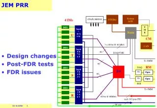
PRR on Patch-Panel ASIC9 Dec. 2002 KEK SOS • Overview • LVDS Rx • Variable Delay • BCID • Test Pulse Generator • Control • Radiation tests • Mass-production and inspection
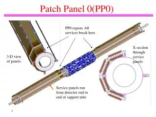
Overview • Requirements • Receives LVDS differential signals from two ASD Boards (2 x 16-ch) • BCID • Variable delays (common for 16-ch signals from a ASD Board) for phase adjustment, variable delays for the clock • Effectively wider gate width than 25 nsec • Variable delays • 25 nsec dynamic range with a step of sub-nano sec. • Two Test Pulse Generators for two ASD Boards with variable amplitude and variable delay • JTAG Control • Process • 0.35 mm full-custom CMOS (Rohm)
LVDS Receiver (I) • Propagation delay vs. amplitude and offset voltage
LVDS Receiver (II) • Dependence on supply voltage
Control via JTAG • BYPASS, No Boundary Scan • TRST_ is not supported. • BCID (Port-A and Port-B) • Mask, Signal Delay, BCID CLK Delay, Gate Width • Test Pulse (Port-A and Port-B) • Amplitude, Fine Delay, Coarse Delay • Debug Variable Delay • SEU flag
Control via input pins • POL • Set whether anode or cathode signals • PLL • ENB, ENV, ENP, SELECT_ENP (test purpose) • STEP0, 1:The number of Delay Units in PLL • STEP decides the dynamic range and a step of the Variable Delay • BCID skip (BYPASS) • Test Pulse Trigger (TPTRG) • RESET_ • Reset all the register to the defaults. • Initiate PLL lock sequence
Radiation Environment (Patch-Panel ASIC) • TID RTC=10.5 krad • SFsim=3.5, SFldr=5, SFlot=2 • RTC=0.3 (Gray/y) x 3.5 x 5 x 2 x 10 years = 105 Gray • Simulated Radiation Level (SRL) for SEE • SRL = 2.11 x 10¹⁰ h/cm2/10years • Rohm 0.35mm CMOS Process • The same process with SLB ASIC • We can deduce the radiation effect from the result of SLB ASICs. • The voting logic is used to all the instruction and data registers.
Radiation Test (TID) • Research Center for Nuclear Science and Technology (RCNST) in Univ. of Tokyo (26 Nov. 02) • 60Co, 0.954 krad/min., 4 samples • 30, 30, 30 and 85 krad • Biased during irradiation • Current measurement • The increase of the current can be observed at more than 30 krad. • Functionality checks before/after irradiation • No functional defect was observed in all 4 chips.
Radiation Test (SEE) • AVF Cyclotron at CYRIC of Tohoku Univ. • Proton beam: E=70 MeV, I=2-4 nA • Beam Fluence and profile using dosimetry • 0.1mm thick Cu foil put on the DUT • Gamma-ray spectra from activated radioisotopes will be measured using a Ge detector. • Intensity distribution of the g-ray will be measured with an Imaging Plate. • 4 ASICs will be tested. • Beam time is 17-18 Dec. (48 hours)
Mass-Production • 10,368 + spares = 15,000 working chips • The re-production of the mask will dominate the price. • Combine the mask and mass-production with other ASICs • JRC ASIC (5 mm x 5 mm, 1600 chips) • SLB ASIC (10 mm x 10 mm, 3000 chips) • Rohm has started their consideration how to proceed the mass-productions. • International Tendering in summer 2003 • Completion of the mass-production by the end of 2003
Inspection • At IC production line (Rohm) • Need negotiations, but they are hesitating. • DC parameters (DC currents) • At KEK • AC measurements • PPGs, FIFO Modules and PT4 modules in VME • Development of a Test Board and software • Comprehensive tests should be done as a PS-Board • 2 [person X month] • Manpower for inspection